Data Sheet
Dual, 10-Bit nanoDAC with 2 ppm/°C Reference, SPI Interface
AD5313R
FEATURES
Low drift 2.5 V reference: 2 p...
Data Sheet
Dual, 10-Bit nanoDAC with 2 ppm/°C Reference, SPI Interface
AD5313R
FEATURES
Low drift 2.5 V reference: 2 ppm/°C typical Tiny package: 3 mm × 3 mm, 16-lead LFCSP Total unadjusted error (TUE): ±0.1% of FSR maximum Offset error: ±1.5 mV maximum Gain error: ±0.1% of FSR maximum High drive capability: 20 mA, 0.5 V from supply rails User selectable gain of 1 or 2 (GAIN pin) Reset to zero scale or midscale (RSTSEL pin) 1.8 V logic compatibility 50 MHz SPI with readback or daisy chain Low glitch: 0.5 nV-sec Low power: 3.3 mW at 3 V 2.7 V to 5.5 V power supply −40°C to +105°C temperature range
APPLICATIONS
Optical transceivers Base station power
amplifiers Process control (PLC I/O cards) Industrial automation Data acquisition systems
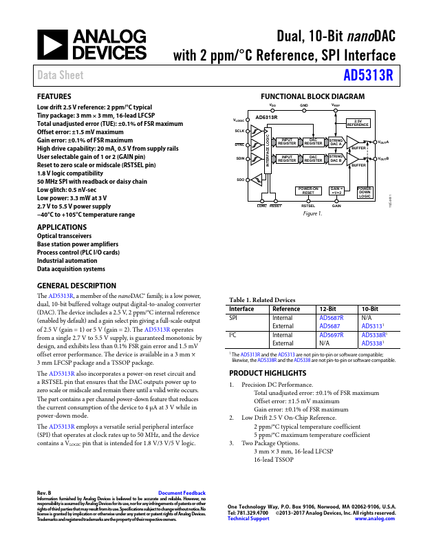
GENERAL DESCRIPTION
The AD5313R, a member of the nanoDAC® family, is a low power, dual, 10-bit buffered
voltage output digital-to-analog converter (DAC). The device includes a 2.5 V, 2 ppm/°C internal reference (enabled by default) and a gain select pin giving a full-scale output of 2.5 V (gain = 1) or 5 V (gain = 2). The AD5313R operates from a single 2.7 V to 5.5 V supply, is guaranteed monotonic by design, and exhibits less than 0.1% FSR gain error and 1.5 mV offset error performance. The device is available in a 3 mm × 3 mm LFCSP package and a TSSOP package.
The AD5313R also incorporates a power-on reset circuit and a RSTSEL pin that ensures that the DAC outputs power up to zero scale or midscale and remain there until a valid write occu...