a
FEATURES Complete Current Output Converter High Stability Buried Zener Reference Laser Trimmed to High Accuracy (1/4 L...
a
FEATURES Complete Current Output Converter High Stability Buried Zener Reference Laser Trimmed to High Accuracy (1/4 LSB Max Error, AD561K, T) Trimmed Output Application Resistors for 0 V to +10 V, ؎5 V Ranges Fast Settling – 250 ns to 1/2 LSB Guaranteed Monotonicity Over Full Operating Temperature Range TTL/DTL and
CMOS Compatible (Positive True Logic) Single Chip Monolithic Construction Available in Chip Form MlL-STD-883-Compliant Versions Available PRODUCT DESCRIPTION
Low Cost 10-Bit Monolithic D/A Converter AD561
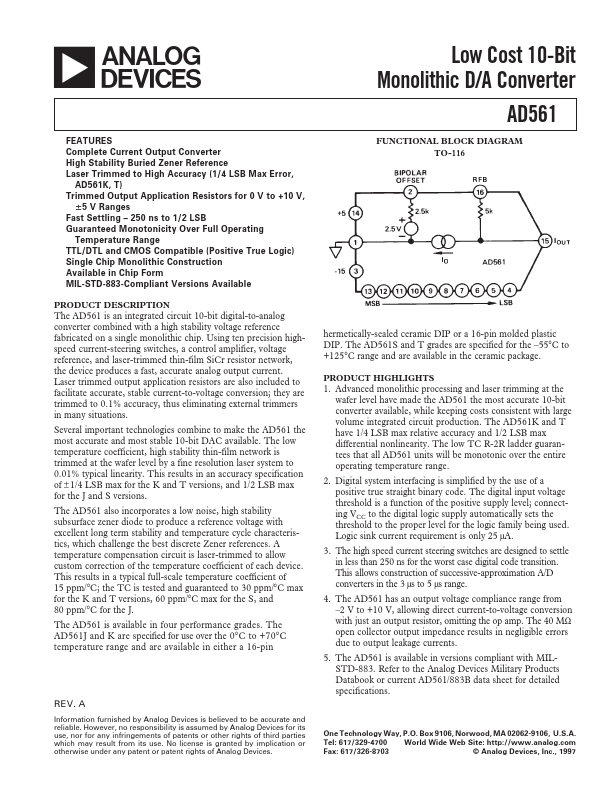
FUNCTIONAL BLOCK DIAGRAM TO-116
The AD561 is an integrated circuit 10-bit digital-to-analog converter combined with a high stability
voltage reference fabricated on a single monolithic chip. Using ten precision highspeed current-steering switches, a control amplifier,
voltage reference, and laser-trimmed thin-film SiCr resistor network, the device produces a fast, accurate analog output current. Laser trimmed output application resistors are also included to facilitate accurate, stable current-to-
voltage conversion; they are trimmed to 0.1% accuracy, thus eliminating external trimmers in many situations. Several important technologies combine to make the AD561 the most accurate and most stable 10-bit DAC available. The low temperature coefficient, high stability thin-film network is trimmed at the wafer level by a fine resolution laser system to 0.01% typical linearity. This results in an accuracy specification of ± 1/4 LSB max for the K and T versions, and 1...