www.DataSheet4U.com
Preliminary Technical Data
FEATURES
Throughput: 6 MSPS SAR architecture 16-bit resolution with no m...
www.DataSheet4U.com
Preliminary Technical Data
FEATURES
Throughput: 6 MSPS SAR architecture 16-bit resolution with no missing codes SNR: 92 dB Typ, 90dB Min @ 1MHz INL: ±1 LSB Typ, ±2 LSB Max DNL: ±0.3 LSB Typ, ±1 LSB Max Differential input range: ± 4.096V No latency/no pipeline delay (SAR architecture) Serial LVDS interface: Self-clocked mode Echoed-clock mode Reference: Internal 4.096 V External (1.2V) buffered to 4.096 V External 4.096 V Power dissipation 150 mW 32-Lead LFCSP package (5 mm x 5 mm)
16-Bit, 6MSPS PulSAR Differential ADC AD7625
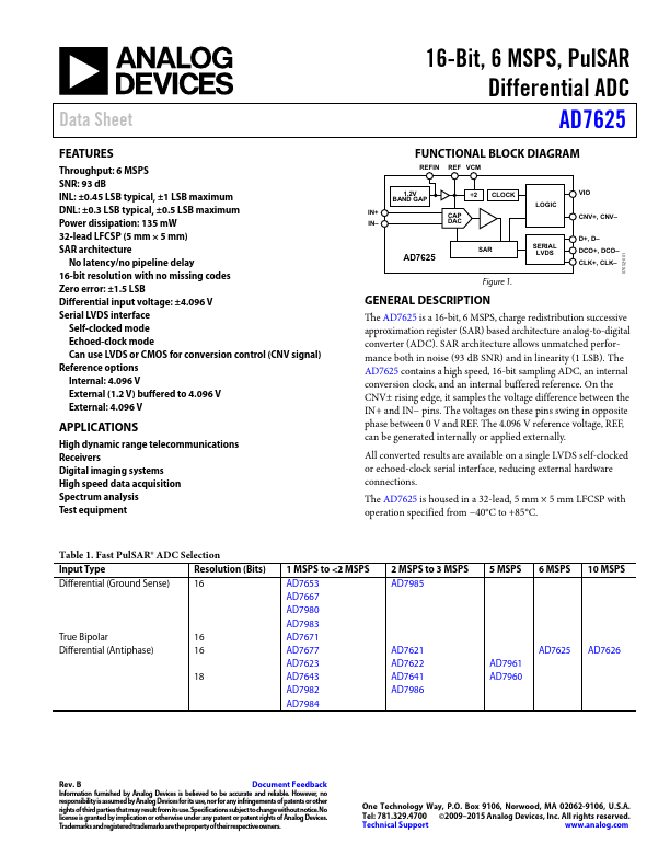
FUNCTIONAL BLOCK DIAGRAM
REFIN REF VCM
1.2V BANDGAP IN+ INCAP DAC
2
CLOCK LOGIC
VIO
CNV
D AD7626 SAR SERIAL LVDS DCO CLK
Figure 1.
GENERAL DESCRIPTION
The AD7625 is a 16-bit, 6MSPS, charge redistribution successive approximation register (SAR) architecture, analog-to-digital converter (ADC). SAR architecture allows unmatched performance both in noise – 92dB SNR - and in linearity – 1LSB. The AD7625 contains a high speed 16-bit sampling ADC, an internal conversion clock, and an internal buffered reference. On the CNV edge, it samples the
voltage difference between IN+ and IN− pins. The
voltages on these pins swing in opposite phase between 0 V and REF. The 4.096V reference
voltage, REF, can be generated internally or applied externally. All converted results are available on a single LVDS self-clocked or echoed-clock serial interface reducing external hardware connections.
APPLICATIONS
High dynamic range telecommunications Re...