Data Sheet
1.2 GHz Clock Distribution IC, PLL Core, Dividers, Delay Adjust, Eight Outputs AD9510
FEATURES
Low phase no...
Data Sheet
1.2 GHz Clock Distribution IC, PLL Core, Dividers, Delay Adjust, Eight Outputs AD9510
FEATURES
Low phase noise phase-locked loop core Reference input frequencies to 250 MHz Programmable dual modulus prescaler Programmable charge pump (CP) current Separate CP supply (VCPS) extends tuning range
Two 1.6 GHz, differential clock inputs 8 programmable dividers, 1 to 32, all integers Phase select for output-to-output coarse delay adjust 4 independent 1.2 GHz LVPECL outputs
Additive output jitter of 225 fs rms 4 independent 800 MHz low
voltage differential signaling
(LVDS) or 250 MHz complementary metal oxide conductor (
CMOS) clock outputs Additive output jitter of 275 fs rms Fine delay adjust on 2 LVDS/
CMOS outputs Serial control port Space-saving 64-lead LFCSP
APPLICATIONS
Low jitter, low phase noise clock distribution Clocking high speed ADCs, DACs, DDSs, DDCs, DUCs, and
mixed-signal front ends (MxFEs) High performance wireless transceivers High performance instrumentation Broadband infrastructure
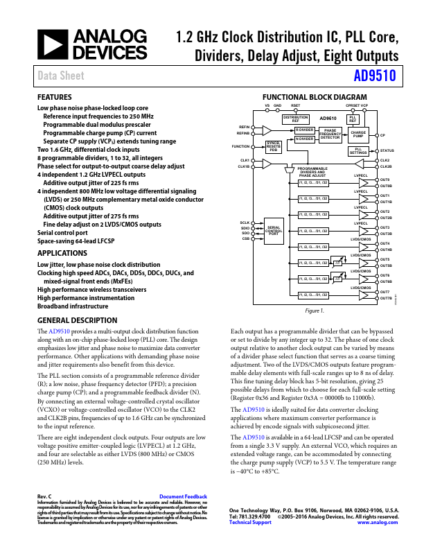
GENERAL DESCRIPTION
The AD9510 provides a multi-output clock distribution function along with an on-chip phase-locked loop (PLL) core. The design emphasizes low jitter and phase noise to maximize data converter performance. Other applications with demanding phase noise and jitter requirements also benefit from this device.
The PLL section consists of a programmable reference divider (R); a low noise, phase frequency detector (PFD); a precision charge pump (CP); and a program...