www.DataSheet4U.com
1.8 V, 12-LVDS/24-CMOS Output, Low Power Clock Fanout Buffer ADCLK854
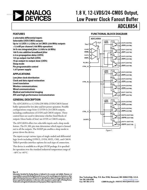
FUNCTIONAL BLOCK DIAGRAM
ADCL...
www.DataSheet4U.com
1.8 V, 12-LVDS/24-
CMOS Output, Low Power Clock Fanout Buffer ADCLK854
FUNCTIONAL BLOCK DIAGRAM
ADCLK854
VREF CLK0 CLK0 CLK1 CLK1 IN_SEL CTRL_A LVDS/
CMOS VS/2 LVDS/
CMOS OUT0 (OUT0A) OUT0 (OUT0B) OUT1 (OUT1A) OUT1 (OUT1B) OUT2 (OUT2A) OUT2 (OUT2B) OUT3 (OUT3A) OUT3 (OUT3B)
FEATURES
2 selectable differential inputs Selectable LVDS/
CMOS outputs Up to 12 LVDS (1.2 GHz) or 24
CMOS (250 MHz) outputs <12 mW per channel (100 MHz operation) 54 fs rms integrated jitter (12 kHz to 20 MHz) 100 fs rms additive broadband jitter 2.0 ns propagation delay (LVDS) 135 ps output rise/fall (LVDS) 70 ps output-to-output skew (LVDS) Sleep mode Pin programmable control 1.8 V power supply
APPLICATIONS
Low jitter clock distribution Clock and data signal restoration Level translation Wireless communications Wired communications Medical and industrial imaging ATE and high performance instrumentation
CTRL_B
OUT4 (OUT4A) OUT4 (OUT4B) OUT5 (OUT5A) OUT5 (OUT5B) OUT6 (OUT6A) OUT6 (OUT6B) OUT7 (OUT7A) OUT7 (OUT7B)
GENERAL DESCRIPTION
The ADCLK854 is a 1.2 GHz/250 MHz LVDS/
CMOS fanout buffer optimized for low jitter and low power operation. Possible configurations range from 12 LVDS to 24
CMOS outputs, including combinations of LVDS and
CMOS outputs. Three control lines are used to determine whether fixed blocks of outputs (three banks of four) are LVDS or
CMOS outputs. The ADCLK854 offers two selectable inputs and a sleep mode feature. The IN_SEL pin state determines which input is f...