www.DataSheet4U.com
Ultrafast, SiGe, Open-Collector HVDS Clock/Data Buffer ADCLK914
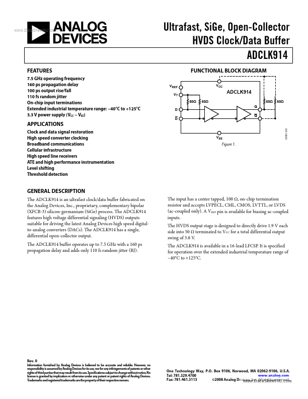
FUNCTIONAL BLOCK DIAGRAM
VREF VT 50...
www.DataSheet4U.com
Ultrafast, SiGe, Open-Collector HVDS Clock/Data Buffer ADCLK914
FUNCTIONAL BLOCK DIAGRAM
VREF VT 50Ω D D 50Ω Q Q VCC
FEATURES
7.5 GHz operating frequency 160 ps propagation delay 100 ps output rise/fall 110 fs random jitter On-chip input terminations Extended industrial temperature range: −40°C to +125°C 3.3 V power supply (VCC − VEE)
ADCLK914
50Ω 50Ω
APPLICATIONS
Clock and data signal restoration High speed converter clocking Broadband communications Cellular infrastructure High speed line receivers ATE and high performance instrumentation Level shifting Threshold detection
VEE
06561-001
Figure 1.
GENERAL DESCRIPTION
The ADCLK914 is an ultrafast clock/data buffer fabricated on the Analog Devices, Inc., proprietary, complementary bipolar (XFCB-3) silicon-germanium (SiGe) process. The ADCLK914 features high
voltage differential signaling (HVDS) outputs suitable for driving the latest Analog Devices high speed digitalto-analog converters (DACs). The ADCLK914 has a single, differential open-collector output. The ADCLK914 buffer operates up to 7.5 GHz with a 160 ps propagation delay and adds only 110 fs random jitter (RJ). The input has a center tapped, 100 Ω, on-chip termination resistor and accepts LVPECL, CML,
CMOS, LVTTL, or LVDS (ac-coupled only). A VREF pin is available for biasing ac-coupled inputs. The HVDS output stage is designed to directly drive 1.9 V each side into 50 Ω terminated to VCC for a total differential output swing of 3.8 V. The AD...