Data Sheet
1.5 Ω On Resistance, ±15 V/12 V/±5 V, iCMOS, Dual SPDT Switch
ADG1436
FEATURES
1.5 Ω on resistance 0.3 Ω on...
Data Sheet
1.5 Ω On Resistance, ±15 V/12 V/±5 V, i
CMOS, Dual SPDT Switch
ADG1436
FEATURES
1.5 Ω on resistance 0.3 Ω on-resistance flatness 0.1 Ω on-resistance match between channels Continuous current per channel
LFCSP package: up to 400 mA TSSOP package: up to 260 mA Fully specified at +12 V, ±15 V, and ±5 V No VL supply required 3 V logic-compatible inputs Rail-to-rail operation 16-lead TSSOP and 4 mm × 4 mm, 16-lead LFCSP packages
APPLICATIONS
Automatic test equipment Data acquisition systems Battery-powered systems Sample-and-hold systems Audio signal routing Communication systems Relay replacement
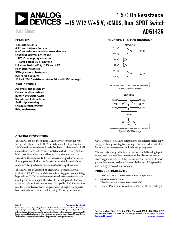
FUNCTIONAL BLOCK DIAGRAMS
ADG1436
S1A D1
S1B
IN1
IN2
S2A D2
S2B
06817-001
SWITCHES SHOWN FOR A ONE-INPUT LOGIC.
Figure 1. TSSOP Package
ADG1436
S1A
S2A
D1
D2
S1B
S2B
LOGIC
GENERAL DESCRIPTION
The ADG1436 is a monolithic
CMOS device containing two independently selectable SPDT switches. An EN input on the LFCSP package enables or disable the device. When disabled, all channels are switched off. Each switch conducts equally well in both directions when on and has an input signal range that extends to the supplies. In the off condition, signal levels up to the supplies are blocked. Both switches exhibit break-beforemake switching action for use in multiplexer applications.
The ADG1436 is designed on an i
CMOS® process. i
CMOS (industrial-
CMOS) is a modular manufacturing process combining high
voltage CMOS (complementary metal-oxide semiconductor) and bipolar technologi...