Data Sheet
FEATURES
2.3 V to 5.5 V input voltage range Output voltage levels (VDDA and VDDB to VSS ≤ 35 V)
Low output vo...
Data Sheet
FEATURES
2.3 V to 5.5 V input
voltage range Output
voltage levels (VDDA and VDDB to VSS ≤ 35 V)
Low output
voltage levels: down to −24.2 V High output
voltage levels: up to +35 V Rise/fall time: 12 ns/19.5 ns typical Propagation delay: 80 ns typical Operating frequency: 100 kHz typical Ultralow quiescent current: 65 μA typical 20-lead, Pb-free, TSSOP package
APPLICATIONS
Low
voltage to high
voltage translation TFT-LCD panels Piezoelectric motor drivers
GENERAL DESCRIPTION
The ADG3123 is an 8-channel, noninverting
CMOS to high
voltage level translator. Fabricated on an enhanced LC2MOS process, the device is capable of operating at high supply
voltages while maintaining ultralow power consumption.
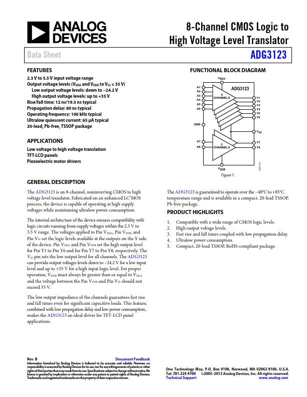
The internal architecture of the device ensures compatibility with logic circuits running from supply
voltages within the 2.3 V to 5.5 V range. The
voltages applied to Pin VDDA, Pin VDDB, and Pin VSS set the logic levels available at the outputs on the Y side of the device. Pin ...