www.DataSheet4U.com
a
Preliminary Technical Data
FEATURES
Voltage-Controlled Amplifier/Attenuator Operating Frequency 1...
www.DataSheet4U.com
a
Preliminary Technical Data
FEATURES
Voltage-Controlled Amplifier/Attenuator Operating Frequency 1 MHz to 3 GHz Optimized for Controlling Output Power High Linearity: OIP3 31 dBm @ 900 MHz Output Noise Floor -150 dBm/Hz @ 900 MHz Fully-Balanced Differential Signal Path Differential Input at 50 Ω Wide Gain-Control Range: -34 dB to +22 dB @ 900 MHz Linear-in-dB Gain Control Function, 20 mV/dB Single Supply 4.75 – 6 V
GAIN
ENBL
1 MHz - 3 GHz VGA with 60dB Gain Control Range ADL5330
VPS2
VPS2
VPS2
VPS2 VPS2
VPS1
GAIN CONTROL
COM1
COM2
RF I/P RF input, 50Ω
INHI INLO
Input gm Stage
Continuously Variable Attenuator
O/P OPHI (TZ) Stage OPLO
BALUN
RF to PA
COM1
APPLICATIONS
Output Power Control for Wireless Infrastructure
BIAS & VREF
COM2
VPS1
VREF
VPS2
IPBS
OPBS
COM2
COM2
COM2
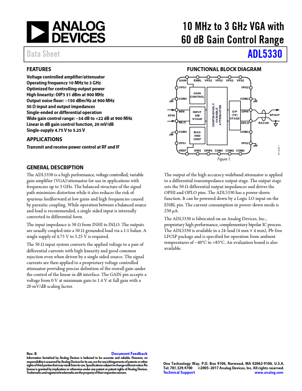
Figure 1. Functional Block Diagram
PRODUCT DESCRIPTION
The ADL5330 is a high-performance
voltage-controlled variablegain amplifier/attenuator, for use up to 3 GHz. The signal path is fully differential; the balanced structure minimizes distortion, and reduces the risk of spurious feed-forward at low gains and high frequencies due to substrate coupling. While operation between a balanced source and load is recommended, a single-sided input is internally converted to differential from. The input impedance is 50-Ω from INHI to INLO. The outputs will usually be coupled into a 50-Ω grounded load via a 1:1 balun. However, the output pins, OPHI and OPLO, may also be us...