Multirate to 2.7 Gb/s Clock and Data Recovery IC with Integrated Limiting Amp ADN2819
FEATURES
Meets SONET requirements ...
Multirate to 2.7 Gb/s Clock and Data Recovery IC with Integrated Limiting Amp ADN2819
FEATURES
Meets SONET requirements for jitter transfer/generation/tolerance Quantizer sensitivity: 4 mV typical Adjustable slice level: ±100 mV 1.9 GHz minimum bandwidth Patented clock recovery architecture Loss of signal detect range: 3 mV to 15 mV Single reference clock frequency for all rates, including 15/14 (7%) wrapper rate Choice of 19.44 MHz, 38.88 MHz, 77.76 MHz, or 155.52 MHz REFCLK LVPECL/LVDS/LV
CMOS/LVTTL compatible inputs (LVPECL/LVDS only at 155.52 MHz) 19.44 MHz oscillator on-chip to be used with external crystal Loss of lock indicator Loopback mode for high speed test data Output squelch and bypass features Single-supply operation: 3.3 V Low power: 540 mW typical 7 mm × 7 mm 48-lead LFCSP
PRODUCT DESCRIPTION
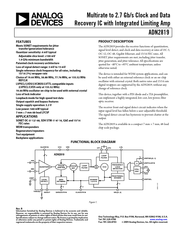
The ADN2819 provides the receiver functions of quantization, signal level detect, and clock and data recovery at rates of OC-3, OC-12, OC-48, Gigabit Ethernet, and 15/14 FEC rates. All SONET jitter requirements are met, including jitter transfer, jitter generation, and jitter tolerance. All specifications are quoted for –40°C to +85°C ambient temperature, unless otherwise noted. The device is intended for WDM system applications, and can be used with either an external reference clock or an on-chip oscillator with external crystal. Both native rates and 15/14 rate digital wrappers are supported by the ADN2819, without any change of reference clock. This device, together w...