Data Sheet
Logic Controlled, High-Side Power Switch with Reverse Current Blocking ADP195
FEATURES
Ultralow on resistan...
Data Sheet
Logic Controlled, High-Side Power Switch with Reverse Current Blocking ADP195
FEATURES
Ultralow on resistance (RDSON) 50 mΩ @ 3.6 V 55 mΩ @ 2.5 V 65 mΩ @ 1.8 V 100 mΩ @ 1.2 V Input
voltage range: 1.1 V to 3.6 V 1.1 A maximum continuous operating current Low enable control logic threshold can be operated from
1.2 V to 3.3 V Low 1 μA (typical) ground current @ 1.8 V Low 4 μA (maximum) reverse current @ 3.6 V Ultralow shutdown current: 0.7 μA (typical) @ 1.8 V Reverse current blocking Tiny 4-ball wafer level chip scale package (WLCSP)
1.0 mm × 1.0 mm, 0.5 mm pitch Tiny 6-lead lead frame chip scale package (LFCSP)
2.0 mm × 2.0 mm × 0.55 mm, 0.65 mm pitch
APPLICATIONS
Mobile phones Digital cameras and audio devices GPS devices Personal media players Portable and battery-powered equipment
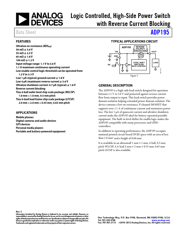
TYPICAL APPLICATIONS CIRCUIT
VIN + – GND
ADP195
REVERSE POLARITY PROTECTION
VOUT
ON EN OFF
LEVEL SHIFT AND SLEW
RATE CONTROL
LOAD
08679-001
Figure 1.
GENERAL DESCRIPTION
The ADP195 is a high-side load switch designed for operation between 1.1 V to 3.6 V and protected against reverse current flow from output to input. This load switch provides power domain isolation helping extended power domain isolation. The device contains a low on-resistance, P-channel
MOSFET that supports over 1.1 A of continuous current and minimizes power loss. The low 1 μA of quiescent current and ultralow shutdown current make the ADP195 ideal for battery-operated portable equipment. The built-in le...