Data Sheet
FEATURES
Low RDSON: 10 mΩ (WLCSP) or 27 mΩ (LFCSP) Wide input voltage range: 1.8 V to 5.5 V Quick output disc...
Data Sheet
FEATURES
Low RDSON: 10 mΩ (WLCSP) or 27 mΩ (LFCSP) Wide input
voltage range: 1.8 V to 5.5 V Quick output discharge (QOD) circuit (ADP196-01) 3 A continuous operating current to 70°C 1.2 V logic-compatible enable input Low 25 μA quiescent current, VIN = 1.8 V Low 40 μA quiescent current, VIN = 5.5 V Overtemperature and overcurrent protection Ultralow shutdown current: <1 μA Ultrasmall 1.0 mm × 1.5 mm, 0.5 mm pitch, 6-ball WLCSP Tiny 2.0 mm × 2.0 mm × 0.55 mm, 0.65 mm pitch, 6-lead LFCSP
5 V, 3 A, Logic Controlled High-Side Power Switch ADP196
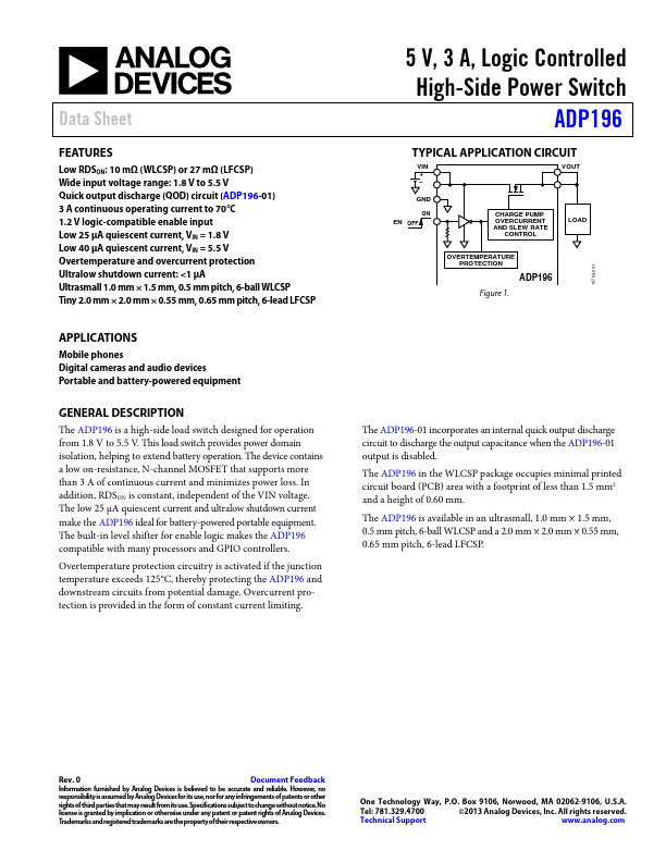
TYPICAL APPLICATION CIRCUIT
VIN + – GND
ON
VOUT
EN OFF
CHARGE PUMP OVERCURRENT AND SLEW RATE CONTROL
LOAD
ADP196
Figure 1.
APPLICATIONS
Mobile phones Digital cameras and audio devices Portable and battery-powered equipment
GENERAL DESCRIPTION
The ADP196 is a high-side load switch designed for operation from 1.8 V to 5.5 V. This load switch provides power domain isolation, helping to extend battery operation. The device contains a low on-resistance, N-channel
MOSFET that supports more than 3 A of continuous current and minimizes power loss. In addition, RDSON is constant, independent of the VIN
voltage. The low 25 μA quiescent current and ultralow shutdown current make the ADP196 ideal for battery-powered portable equipment. The built-in level shifter for enable logic makes the ADP196 compatible with many processors and GPIO controllers. Overtemperature protection circuitry is activated if the junction temperature exceed...