a
FEATURES Wide Input Voltage Range: 3.6 V to 30 V Adjustable and Fixed (3.3 V, 5 V) Output Options Integrated 1 A Power...
a
FEATURES Wide Input
Voltage Range: 3.6 V to 30 V Adjustable and Fixed (3.3 V, 5 V) Output Options Integrated 1 A Power Switch Uses Small Surface-Mount Components Cycle-By-Cycle Current Limiting Peak Input
Voltage (100 ms): 60 V Thermally Enhanced 8-Lead SOIC Package Configurable as a Buck, Buck-Boost and SEPIC Regulator APPLICATIONS Industrial Power Systems PC Peripheral Power Systems Preregulator for Linear Regulators Distributed Power Systems Automotive Systems Battery Chargers
200 kHz, 1 A High-
Voltage Step-Down Switching Regulator ADP3050
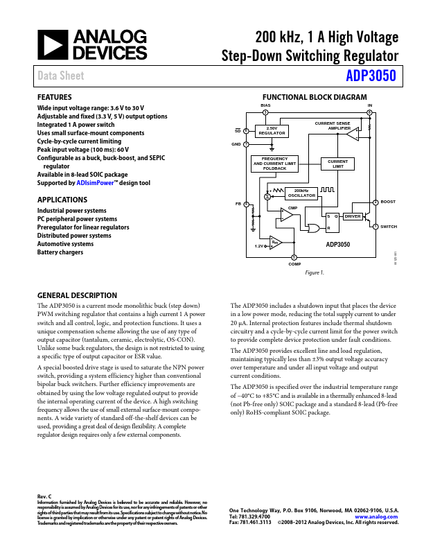
FUNCTIONAL BLOCK DIAGRAM
BIAS IN CURRENT SENSE AMPLIFIER
SD GND
2.5V REGULATOR
FREQUENCY AND CURRENT LIMIT FOLDBACK
CURRENT LIMIT
+
200kHz OSCILLATOR BOOST CMP S R gm Q DRIVER SWITCH
FB
1.2V
ADP3050
COMP
GENERAL DESCRIPTION
The ADP3050 is a current-mode monolithic buck (step-down) PWM switching regulator that contains a high current 1 A power switch and all control, logic, and protection functions. It uses a unique compensation scheme that allows the use of any type of output capacitor (tantalum, ceramic, electrolytic, OS-CON). Unlike some buck regulators, the design is not restricted to using a specific type of output capacitor or ESR value. A special boosted drive stage is used to saturate the NPN power switch, providing a system efficiency higher than conventional bipolar buck switchers. Further efficiency improvements are obtained by using the low
voltage regulated output to provide the device's internal operating curr...