Dual, Bootstrapped, 12 V MOSFET Driver with Output Disable ADP3650
FEATURES
All-in-one synchronous buck driver Bootstrap...
Dual, Bootstrapped, 12 V
MOSFET Driver with Output Disable ADP3650
FEATURES
All-in-one synchronous buck driver Bootstrapped high-side drive One PWM signal generates both drives Anti-crossconduction protection circuitry OD for disabling the driver outputs
GENERAL DESCRIPTION
The ADP3650 is a dual, high
voltage MOSFET driver optimized for driving two N-channel
MOSFETs, the two switches in a nonisolated synchronous buck power converter. Each driver is capable of driving a 3000 pF load with a 45 ns propagation delay and a 25 ns transition time. One of the drivers can be bootstrapped and is designed to handle the high
voltage slew rate associated with floating high-side gate drivers. The ADP3650 includes overlapping drive protection to prevent shoot-through current in the external
MOSFETs. The OD pin shuts off both the high-side and the low-side
MOSFETs to prevent rapid output capacitor discharge during system shutdown. The ADP3650 is specified over the temperature range of −40°C to +85°C and is available in 8-lead SOIC_N and 8-lead LFCSP_VD packages.
APPLICATIONS
Telecom and datacom networking Industrial and medical systems Point of load conversion: memory, DSP, FPGA, ASIC
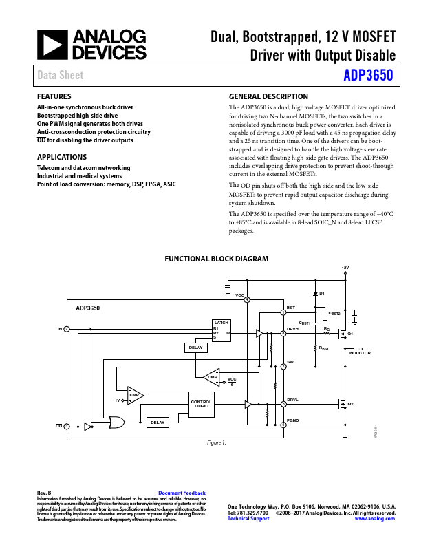
FUNCTIONAL BLOCK DIAGRAM
12V
VCC
D1
4
ADP3650
LATCH R1 R2 Q S DELAY
BST
1
CBST2 CBST1 DRVH RG
IN 2
8
Q1 TO INDUCTOR
RBST SW
7
CMP
VCC 6 DRVL
5
CMP 1V CONTROL LOGIC
Q2
Figure 1.
Rev. A
Information furnished by Analog Devices is believed to be accurate and reliable. However, no responsibility is...