Data Sheet
1 A/0.6 A, DC-to-DC Switching Regulator with Independent Positive and Negative Outputs
ADP5070
FEATURES
Wi...
Data Sheet
1 A/0.6 A, DC-to-DC Switching Regulator with Independent Positive and Negative Outputs
ADP5070
FEATURES
Wide input supply
voltage range: 2.85 V to 15 V Generates well regulated, independently resistor
programmable VPOS and VNEG outputs Boost regulator to generate VPOS output
Adjustable positive output to 39 V Integrated 1.0 A main switch Optional single-ended primary-inductor converter (SEPIC)
configuration for automatic step-up/step-down Inverting regulator to generate VNEG output
Adjustable negative output to VIN − 39 V Integrated 0.6 A main switch True shutdown for both positive and negative outputs 1.2 MHz/2.4 MHz switching frequency with optional external frequency synchronization from 1.0 MHz to 2.6 MHz Resistor programmable soft start timer Slew rate control for lower system noise Individual precision enable and flexible start-up sequence control for symmetric start, VPOS first, or VNEG first Out-of-phase operation UVLO, OCP, OVP, and TSD protection 4 mm × 4 mm, 20-lead LFCSP and 20-lead TSSOP −40°C to +125°C junction temperature range Supported by the ADIsimPower tool set
APPLICATIONS
Bipolar
amplifiers, ADCs, DACs and multiplexers Charge-coupled device (CCD) bias supply Optical module supply RF power amplifier (PA) bias
GENERAL DESCRIPTION
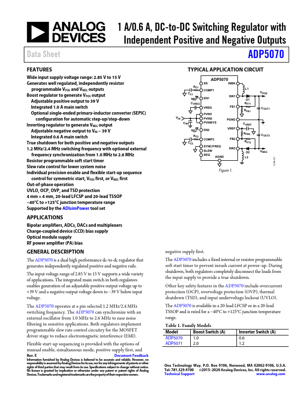
The ADP5070 is a dual high performance dc-to-dc regulator that generates independently regulated positive and negative rails.
The input
voltage range of 2.85 V to 15 V supports a wide variety of applications. The...