Product Folder
Sample & Buy
Technical Documents
Tools & Software
Support & Community
ADS4229
SBAS550C – JUNE 2011 –...
Product Folder
Sample & Buy
Technical Documents
Tools & Software
Support & Community
ADS4229
SBAS550C – JUNE 2011 – REVISED MAY 2015
ADS4229 Dual-Channel, 12-Bit, 250-MSPS Ultralow-Power ADC
1 Features
1 Maximum Sample Rate: 250 MSPS Ultralow Power with Single 1.8-V Supply:
– 545-mW Total Power at 250 MSPS High Dynamic Performance:
– 80.8-dBc SFDR at 170 MHz – 69.4-dBFS SNR at 170 MHz Crosstalk: > 90 dB at 185 MHz Programmable Gain Up to 6 dB for SNR and SFDR Trade-off DC Offset Correction Output Interface Options: – 1.8-V Parallel
CMOS Interface – DDR LVDS With Programmable Swing:
– Standard Swing: 350 mV – Low Swing: 200 mV Supports Low Input Clock Amplitude Down to 200 mVPP Package: 9-mm × 9-mm, 64-Pin Quad Flat No-Lead (QFN) Package
3 Description
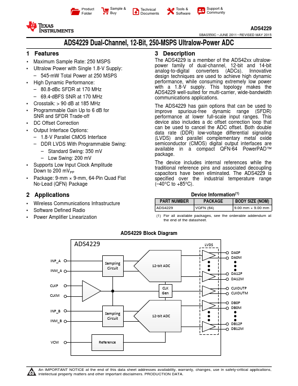
The ADS4229 is a member of the ADS42xx ultralowpower family of dual-channel, 12-bit and 14-bit analog-to-digital converters (ADCs). Innovative design techniques are used to achieve high dynamic performance, while consuming extremely low power with a 1.8-V supply. This topology makes the ADS4229 well-suited for multi-carrier, wide-bandwidth communications applications.
The ADS4229 has gain options that can be used to improve spurious-free dynamic range (SFDR) performance at lower full-scale input ranges. This device also includes a dc offset correction loop that can be used to cancel the ADC offset. Both double data rate (DDR) low-
voltage differential signaling (LVDS) and parallel complementary metal oxide ...