ADS62PF49
www.ti.com
Dual-Channel, 250-MSPS Feedback Receiver IC
Check for Samples: ADS62PF49
SLAS779 – JUNE 2011
FE...
ADS62PF49
www.ti.com
Dual-Channel, 250-MSPS Feedback Receiver IC
Check for Samples: ADS62PF49
SLAS779 – JUNE 2011
FEATURES
1
Maximum Output Sample Rate: 250 MSPS Pin-Compatible with ADS62P49 Variable Output Resolution
– High Resolution Burst Mode with 14-Bit Output: 73 dB SNR at Low IF, 70.5 dB SNR at 170 MHz
– Low Resolution with 9-Bit 250 MSPS or 11-Bit 125 MSPS
Double Data Rate (DDR) LVDS Output Programmable Gain up to 6 dB for SNR/SFDR
Trade-off 90-dB Cross-Talk Power Consumption of 1.25 W 64-Pin QFN Package (9 mm × 9 mm)
APPLICATIONS
Feedpath Path for Multi-Carrier, Multi-Mode Cellular Infrastructure Base Stations
DESCRIPTION
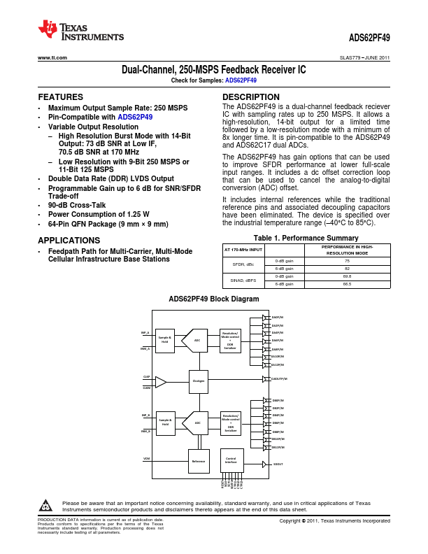
The ADS62PF49 is a dual-channel feedback reciever IC with sampling rates up to 250 MSPS. It allows a high-resolution, 14-bit output for a limited time followed by a low-resolution mode with a minimum of 8x longer time. It is pin-compatible to the ADS62P49 and ADS62C17 dual ADCs.
The ADS62PF49 has gain options that can be used to improve SFDR performance at lower full-scale input ranges. It includes a dc offset correction loop that can be used to cancel the analog-to-digital conversion (ADC) offset.
It includes internal references while the traditional reference pins and associated decoupling
capacitors have been eliminated. The device is specified over the industrial temperature range (–40°C to 85°C).
Table 1. Performance Summary
AT 170-MHz INPUT
PERFORMANCE IN HIGHRESOLUTION MODE
0-dB gain
75
SFDR, dBc
6-dB gain
82
0...