Description
II)
~ ~National
~ ~ Semiconductor
o u~.
voltage gain is internally controlled by the output
signal. The gain control feedback system is AC coupled so that DC signals do not affect the gain.
Features
- Optional gain adjustment - High input impedance
100k
- OdBm output level - Internal reference - Wide supply voltage range - Input level range - Frequency range
±9.0 V to ±18 V +30dBm (2.45Vrms)
500 Hz to 10 kHz
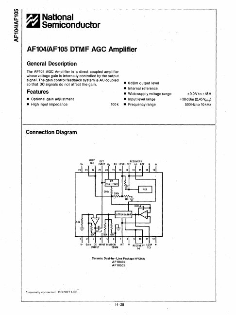
Connection Diagram
LOOP TC2
24
* *V- GAIN DC INPUT DIVIDER INT
RECiiVEiiv LOOP
OUTPUT
CDMM
(+) TCl
Ceramic Dual·ln-line Package HY24A AF104CJ AF105CJ
*Internally connected. DO NOT USE.
14-28
Absolute Maximum Ratings
Supply Voltage Power Dissipation Input Voltage Output Short Circuit Duration Lead Temperature (soldering, 10 sec.) Operating Temperature Range Storage Temperature Range
±18V 1W
±36V Infinite 300°C OoC to +70°C -25°C to +100°C
l>
...
Similar Datasheet
- AF109R PNP GERMANIUM RF TRANSISTOR - Siemens Semiconductor Group
- AF106 PNP GERMANIUM RF TRANSISTOR - Siemens Semiconductor Group
- AF105 DTMF AGC Amplifier - National Semiconductor
- AF103 Low Band Splitter - National Semiconductor
| @ 2014 :: Datasheetspdf.com :: Semiconductors datasheet search & download site. (Privacy Policy & Contact) |