1/3 inch CCD Image Sensor
1
A1 PROs
A1 PROs
Ver1.0
Ai325
1/3 inch CCD Image Sensor for EIA B/W Camera
Description
The Ai325 is a 250K pixels CC...
Description
1
A1 PROs
A1 PROs
Ver1.0
Ai325
1/3 inch CCD Image Sensor for EIA B/W Camera
Description
The Ai325 is a 250K pixels CCD area sensor for EIA 1/3inch video cameras. Buried photodiode and micro lens are adopted for low noise, low smear and high sensitivity. This chip also features a strong anti-blooming and electronic shutter with variable charge-storage time.
Feature
-. Micro Lens for high sensitivity -. Image-lag is negligible and excellent blooming
suppression is performed. -. TTL level(5V) operation on HCCD & RG electrodes. -. 16 pin plastic-DIP. -. Variable electronic shutter of 1/60 to 1/100,000 sec. -. High sensitivity and low smear.
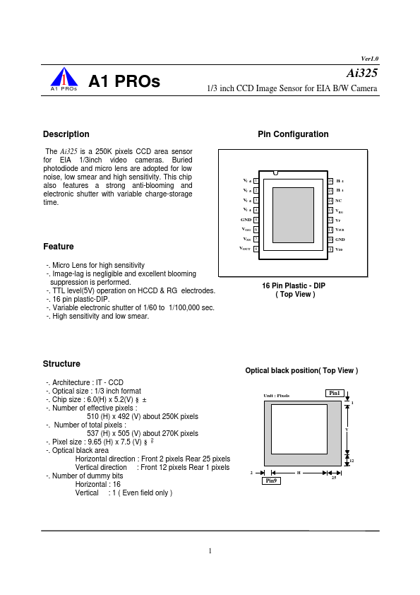
Pin Configuration
V¥ 4õ 1 V¥ 3õ 2 V¥ 2õ 3 V¥ 1õ 4 GND 5 VGG 6 VSS 7 VOUT 8
16 H¥ 2õ 15 H¥ 1õ 14 NC 13 VRG 12 VPP 11 VSUB 10 GND 9 VDD
16 Pin Plastic - DIP ( Top View )
Structure
-. Architecture : IT - CCD -. Optical size : 1/3 inch format -. Chip size : 6.0(H) x 5.2(V) § ± -. Number of effective pixels :
510 (H) x 492 (V) about 250K pixels -. Number of total pixels :
537 (H) x 505 (V) about 270K pixels -. Pixel size : 9.65 (H) x 7.5 (V) § -2 -. Optical black area
Horizontal direction : Front 2 pixels Rear 25 pixels Vertical direction : Front 12 pixels Rear 1 pixels -. Number of dummy bits Horizontal : 16 Vertical : 1 ( Even field only )
Optical black position( Top View )
Unit : Pixels
Pin1
1
V
2
Pin9
H
12 25
1
Block Diagram
VOUT VSS VGG GND V¥ õ1 V¥ õ2 V¥ õ3 V¥ õ4 8 76 54 32 1
PD
Ai325
VCCD
HCCD
Pin Description
9
10 11...
Similar Datasheet