PRELIMINARY
AIC1840/1841
LOW-NOISE, REGULATED GaAsFET BIAS
SPEC NO: DS-1840-P2
! FEATURES
" Low Output Noise: 2mV Ripp...
PRELIMINARY
AIC1840/1841
LOW-NOISE, REGULATED GaAsFET BIAS
SPEC NO: DS-1840-P2
! FEATURES
" Low Output Noise: 2mV Ripple. " Work with Small
Capacitors (as Low as 0.22µF). " Fixed -2V or Adjustable Output. " 2.5V to 6.5V Input
Voltage Range. " Switching Frequency: 104KHz in Normal Operation. " 1µA Maximum in Shutdown Mode.
! APPLICATIONS
" Cellular Phones. " GaAsFET Power Amplifier Modules. " Personal Communicators and PDAs. " Wireless Data Loggers. " LCD Bias Contrast Control. " Regulated Negative Power Supplies.
! DESCRIPTION
The AIC1840/1841 is a switched-capacitor
voltage inverter that generates a regulated fixed -2.0V or externally adjustable output. An internal linear post-regulator reduces the output
voltage ripple to less than 2mV, making the AIC1840/1841 excellent for use as bias
voltage generator for transmitter GaAsFETs in portable RF and cellular telephone applications. The operation
voltage is as low as 2.5V.
The AIC1840/1841 offers a -2V preset output as well as a -1.3V to -3.0V adjustable output. Input
voltage range for AIC1840/1841 is 2.5V to 6.5V. Output current is 5mA at VOUT= -2V and with VIN≥2.5V. Quiescent current is 510µA at VIN=3.6V and reduces to less than 1µA in shutdown mode (3µA max. for the AIC1841).
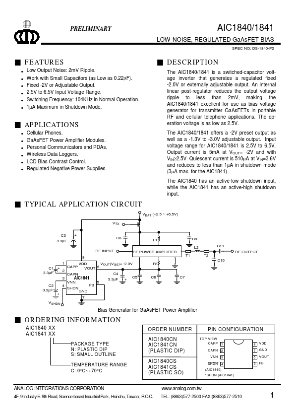
! TYPICAL APPLICATION CIRCUIT
The AIC1840 has an active-low shutdown input, while the AIC1841 has an active-high shutdown input.
VBAT (+2.5 ~ +6.5V) VTX
C3 3.3µF
+
C8 L1
C9
RF INPUT 8
RF POWER AMPLIFIER
L2 T1
C1 3.3µF
+
1 2
VDD CAPP VOU...