AN6555, AN6556, AN6556S
Low Noise Dual Operational Amplifiers
s Overview
The AN6555, the AN6556, and the AN6556S are low...
AN6555, AN6556, AN6556S
Low Noise Dual Operational
Amplifiers
s Overview
The AN6555, the AN6556, and the AN6556S are low noise, high slew rate dual operational
amplifiers with phase compensation circuits built-in. They are suitable for applications to various electronic circuits such as active filters and audio pre
amplifiers.
AN6555
2.4±0.25 3.3±0.25 6.0±0.3 Unit:mm
8
0.5±0.1
7
23.3±0.3
6 5 4
2 1 0.3 – 0.05
+ 0.1
Phase compensation circuit High
voltage gain:Gv=100 dB typ. Low noise:input referred noise
voltage Vni=1.5µ Vrms typ. High slew rate:SR=2V/µ s typ. Output short-circuit protection
3.0±0.3
9-pin SIL Plastic Package (SIP009-P-0000)
AN6556
1.4±0.3 30˚
s Features
1.5±0.25
3
1.5±0.25
2.54
9
Unit:mm
1
9.4±0.3
8 7
2 3 4 6.3±0.3
5 0.51min. 3.8±0.25 (3.45)
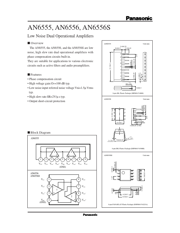
s Block Diagram
AN6555
3—15˚
+ 0.1
7.62±0.25
0.15 – 0.05
8-pin DIL Plastic Package (DIP008-P-0300B)
1 – 1 VCC 2 3 + 4 5 + 6
2 – 7 8 9 VCC
0.6±0.3 0.4±0.25
AN6556S
Unit:mm
VO1 Vin1– Vin1+ VEE Vin2+ Vin2– VO2 (GND)
1 2 3 4
8 7 6 5 5.0±0.3 0.15 0.65 1.5±0.2
VO1 Vin1– Vin1+ VEE (GND)
1 2 3 4 – 1 + 2 + –
8 7 6 5
VCC VO2 Vin2– Vin2+
0.1±0.1
1.27
AN6556 AN6556S
0.3
4.2±0.3 6.5±0.3
8-pin PANAFLAT Plastic Package (SOP008-P-0225A)
2.54
6
0.5±0.1 1.2±0.25
s Pin Descriptions
〈AN6555〉 Pin No. 1 2 3 4 5 6 7 8 9 VCC Ch.1 output Ch.1 inverting input Ch.1 non inverting input VEE (GND) Ch.2 non inverting input Ch.2 inverting input Ch.2 output VCC Pin name 〈AN6556, AN6556S〉 Pin No. 1 2 3 ...