www.DataSheet4U.com
AO3406 N-Channel Enhancement Mode Field Effect Transistor
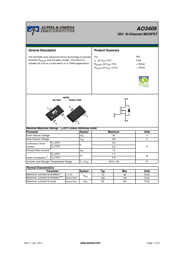
General Description
The AO3406 uses advan...
www.DataSheet4U.com
AO3406 N-Channel Enhancement Mode Field Effect Transistor
General Description
The AO3406 uses advanced trench technology to provide excellent RDS(ON) and low gate charge. This device is suitable for use as a load switch or in PWM applications. Standard Product AO3406 is Pb-free (meets ROHS & Sony 259 specifications). AO3406L is a Green Product ordering option. AO3406 and AO3406L are electrically identical.
Features
VDS (V) = 30V ID = 3.6A (VGS = 10V) RDS(ON) < 65mΩ (VGS = 10V) RDS(ON) < 105mΩ (VGS = 4.5V)
TO-236 (SOT-23) Top View G D S G
D
S
Absolute Maximum Ratings TA=25°C unless otherwise noted Parameter Symbol VDS Drain-Source
Voltage VGS Gate-Source
Voltage Continuous Drain Current A Pulsed Drain Current Power Dissipation A
B
Maximum 30 ±20 3.6 2.9 15 1.4 0.9 -55 to 150
Units V V A
TA=25°C TA=70°C TA=25°C TA=70°C ID IDM PD TJ, TSTG
W °C
Junction and Storage Temperature Range Thermal Characteristics Parameter Maximum Junction-to-Ambient A Maximum Junction-to-Ambient A Maximum Junction-to-Lead C
Symbol t ≤ 10s Steady-State Steady-State RθJA RθJL
Typ 70 100 63
Max 90 125 80
Units °C/W °C/W °C/W
Alpha & Omega Semiconductor, Ltd.
AO3406
Electrical Characteristics (TJ=25°C unless otherwise noted) Symbol Parameter Conditions ID=250µA, VGS=0V VDS=24V, VGS=0V TJ=55°C VDS=0V, VGS=±20V VDS=VGS ID=250µA VGS=10V, VDS=5V VGS=10V, ID=3.6A RDS(ON) gFS VSD IS Static Drain-Source On-Resistance VGS=4.5V, ID=2.8A Forward Transconductance VDS=5V, ID=3.6A ...