August 2002
AO3410 N-Channel Enhancement Mode Field Effect Transistor
General Description
The AO3410 uses advanced tren...
August 2002
AO3410 N-Channel Enhancement Mode Field Effect Transistor
General Description
The AO3410 uses advanced trench technology to provide excellent RDS(ON), low gate charge and operation with gate
voltages as low as 1.8V and as high as 12V. This device is suitable for use as a load switch or in PWM applications.
Features
VDS (V) = 30V ID = 5.8 A RDS(ON) < 28mΩ (VGS = 10V) RDS(ON) < 33mΩ (VGS = 4.5V) RDS(ON) < 52mΩ (VGS = 2.5V) RDS(ON) < 70mΩ (VGS = 1.8V)
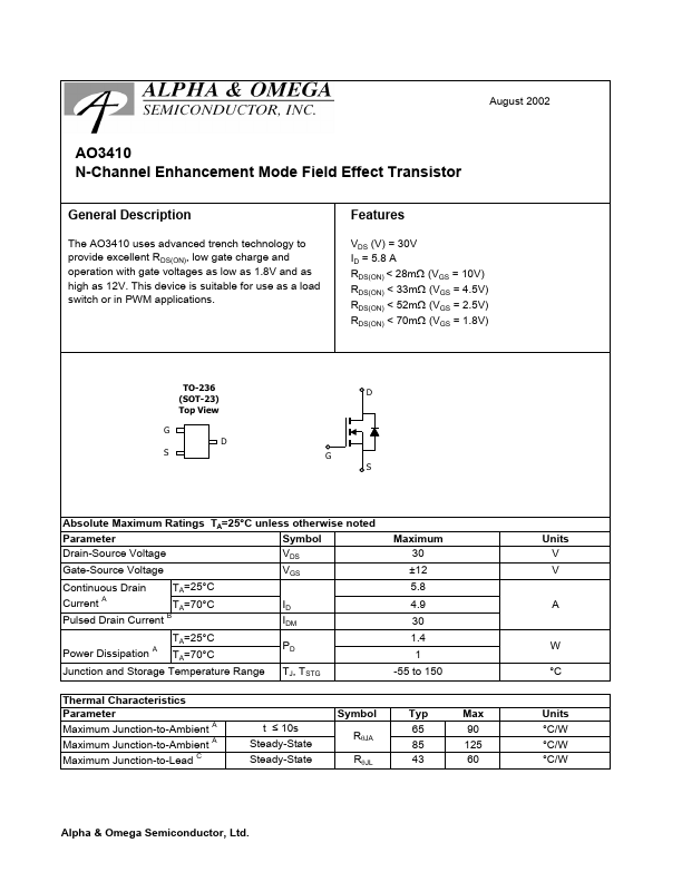
TO-236 (SOT-23) Top View G D S G
D
S
Absolute Maximum Ratings TA=25°C unless otherwise noted Parameter Symbol VDS Drain-Source
Voltage VGS Gate-Source
Voltage Continuous Drain Current A Pulsed Drain Current Power Dissipation A
B
Maximum 30 ±12 5.8 4.9 30 1.4 1 -55 to 150
Units V V A
TA=25°C TA=70°C TA=25°C TA=70°C ID IDM PD TJ, TSTG
W °C
Junction and Storage Temperature Range Thermal Characteristics Parameter Maximum Junction-to-Ambient A Maximum Junction-to-Ambient A Maximum Junction-to-Lead C
Symbol t ≤ 10s Steady-State Steady-State RθJA RθJL
Typ 65 85 43
Max 90 125 60
Units °C/W °C/W °C/W
Alpha & Omega Semiconductor, Ltd.
AO3410
Electrical Characteristics (TJ=25°C unless otherwise noted) Symbol Parameter STATIC PARAMETERS BVDSS Drain-Source Breakdown
Voltage IDSS IGSS VGS(th) ID(ON) Zero Gate
Voltage Drain Current Gate-Body leakage current Gate Threshold
Voltage On state drain current Conditions ID=250µA, VGS=0V VDS=24V, VGS=0V TJ=55°C VDS=0V, VGS=±12V VDS=VGS ID=250µA VGS=4.5V, VDS=5V VGS=10V, ID=5...