Rev 2: Nov 2004
AO3416, AO3416L ( Green Product ) N-Channel Enhancement Mode Field Effect Transistor
General Descripti...
Rev 2: Nov 2004
AO3416, AO3416L ( Green Product ) N-Channel Enhancement Mode Field Effect Transistor
General Description
The AO3416 uses advanced trench technology to provide excellent RDS(ON), low gate charge and operation with gate
voltages as low as 1.8V. This device is suitable for use as a load switch or in PWM applications. It is ESD protected. AO3416L ( Green Product ) is offered in a lead-free package.
Features
VDS (V) = 20V ID = 6.5 A RDS(ON) < 22mΩ (VGS = 4.5V) RDS(ON) < 26mΩ (VGS = 2.5V) RDS(ON) < 34mΩ (VGS = 1.8V) ESD Rating: 2000V HBM
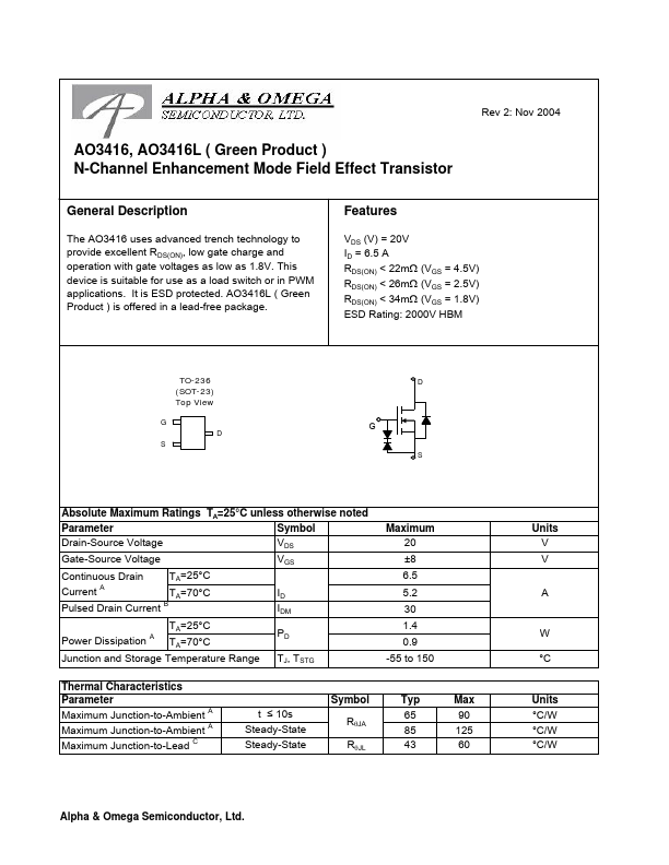
TO-236 (SOT-23) Top View
G D
S
D
G S
Absolute Maximum Ratings TA=25°C unless otherwise noted
Parameter
Symbol
Drain-Source
Voltage
VDS
Gate-Source
Voltage
VGS
Continuous Drain
TA=25°C
Current A
TA=70°C
Pulsed Drain Current B
ID IDM
TA=25°C Power Dissipation A TA=70°C
PD
Junction and Storage Temperature Range TJ, TSTG
Maximum 20 ±8 6.5 5.2 30 1.4 0.9
-55 to 150
Thermal Characteristics
Parameter Maximum Junction-to-Ambient A Maximum Junction-to-Ambient A Maximum Junction-to-Lead C
t ≤ 10s Steady-State Steady-State
Symbol RθJA RθJL
Typ 65 85 43
Max 90 125 60
Units V V
A
W °C
Units °C/W °C/W °C/W
Alpha & Omega Semiconductor, Ltd.
AO3416. AO3416L
Electrical Characteristics (TJ=25°C unless otherwise noted)
Symbol
Parameter
Conditions
STATIC PARAMETERS BVDSS Drain-Source Breakdown
Voltage
IDSS Zero Gate
Voltage Drain Current
ID=250µA, VGS=0V VDS=16V, VGS=0V
IGSS VGS(th) ID(ON)
RDS(ON)
gFS VSD IS
Gate-B...