www.DataSheet4U.com
AO3700 N-Channel Enhancement Mode Field Effect Transistor with Schottky Diode
General Description
T...
www.DataSheet4U.com
AO3700 N-Channel Enhancement Mode Field Effect Transistor with Schottky Diode
General Description
The AO3700 uses advanced trench technology to provide excellent R DS(ON) and low gate charge. A Schottky diode is provided to facilitate the implementation of a bidirectional blocking switch, or for DC-DC conversion applications. Standard Product AO3700 is Pb-free (meets ROHS & Sony 259 specifications). AO3700L is a Green Product ordering option. AO3700 and AO3700L are electrically identical.
Features
VDS (V) = 30V ID = 3.3A (V GS = 10V) RDS(ON) < 65m Ω (VGS = 10V) RDS(ON) < 75m Ω (VGS = 4.5V) RDS(ON) < 160m Ω (VGS = 2.5V) SCHOTTKY VDS (V) = 20V, I F = 1A, VF<
[email protected]
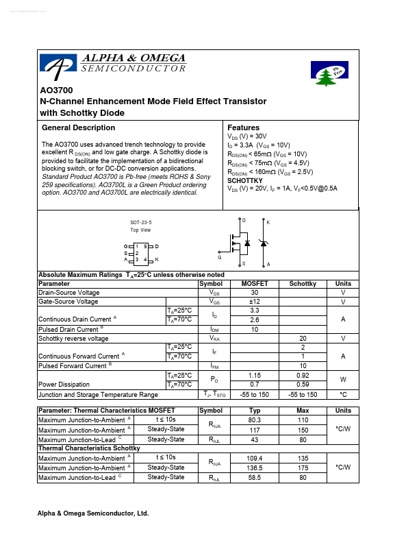
SOT-23-5 Top View G S A 1 2 3 5 4 D K G
D
K
S
A
Absolute Maximum Ratings T A=25°C unless otherwise noted Parameter Symbol VDS Drain-Source
Voltage VGS Gate-Source
Voltage TA=25°C ID Continuous Drain Current A TA=70°C IDM Pulsed Drain Current B VKA Schottky reverse
voltage TA=25°C IF Continuous Forward Current A TA=70°C IFM Pulsed Forward Current B Power Dissipation Junction and Storage Temperature Range Parameter: Thermal Characteristics
MOSFET t ≤ 10s Maximum Junction-to-Ambient A Maximum Junction-to-Ambient A Maximum Junction-to-Lead C Thermal Characteristics Schottky Maximum Junction-to-Ambient Maximum Junction-to-Ambient Maximum Junction-to-Lead C
A A
MOSFET 30 ±12 3.3 2.6 10
Schottky
Units V V A
TA=25°C TA=70°C
PD TJ, TSTG Symbol RθJA RθJL RθJA RθJL
1.15 0.7 -55 to 150 Typ 80....