August 2002
AO4415 P-Channel Enhancement Mode Field Effect Transistor
General Description
www.DataSheet4U.com provide
...
August 2002
AO4415 P-Channel Enhancement Mode Field Effect Transistor
General Description
www.DataSheet4U.com provide
Features
VDS (V) = -30V ID = -8 A RDS(ON) < 26mΩ (VGS = -20V) RDS(ON) < 35mΩ (VGS = -10V)
The AO4415 uses advanced trench technology to excellent RDS(ON), and ultra-low low gate charge. This device is suitable for use as a load switch or in PWM applications.
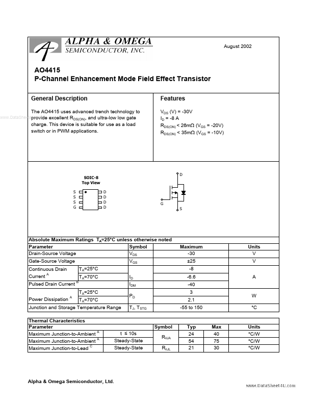
SOIC-8 Top View S S S G D D D D
D
G S
Absolute Maximum Ratings TA=25°C unless otherwise noted Parameter Symbol VDS Drain-Source
Voltage VGS Gate-Source
Voltage Continuous Drain Current A Pulsed Drain Current Power Dissipation A
B
Maximum -30 ±25 -8 -6.6 -40 3 2.1 -55 to 150
Units V V A
TA=25°C TA=70°C TA=25°C TA=70°C ID IDM PD TJ, TSTG
W °C
Junction and Storage Temperature Range Thermal Characteristics Parameter Maximum Junction-to-Ambient A Maximum Junction-to-Ambient A Maximum Junction-to-Lead C
Symbol t ≤ 10s Steady-State Steady-State RθJA RθJL
Typ 24 54 21
Max 40 75 30
Units °C/W °C/W °C/W
Alpha & Omega Semiconductor, Ltd.
AO4415
Electrical Characteristics (TJ=25°C unless otherwise noted) Symbol Parameter STATIC PARAMETERS BVDSS Drain-Source Breakdown
Voltage IDSS IGSS VGS(th) ID(ON)
www.DataSheet4U.com
Conditions ID=-250µA, VGS=0V VDS=-24V, VGS=0V TJ=55°C VDS=0V, VGS=±25V VDS=VGS ID=-250µA VGS=-10V, VDS=-5V VGS=-20V, ID=-8A TJ=125°C VGS=-10V, ID=-8A VGS=-6V, ID=-5A VDS=-5V, ID=-8A
Min -30
Typ
Max
Units V
Zero Gate
Voltage Drain Current Gate-Body leakage current Gate Threshold ...