AO4420A N-Channel Enhancement Mode Field Effect Transistor
General Description
The AO4420A uses advanced trench technolo...
AO4420A N-Channel Enhancement Mode Field Effect Transistor
General Description
The AO4420A uses advanced trench technology to provide excellent R DS(ON), shoot-through immunity and www.DataSheet4U.com body diode characteristics.This device is suitable for use as a synchronous switch in PWM applications. Standard Product AO4420A is Pb-free (meets ROHS & Sony 259 specifications).
Features
VDS (V) = 30V ID = 13.7A (VGS = 10V) RDS(ON) < 10.5mΩ (VGS = 10V) RDS(ON) < 12mΩ (VGS = 4.5V) UIS Tested Rg,Ciss,Coss,Crss Tested
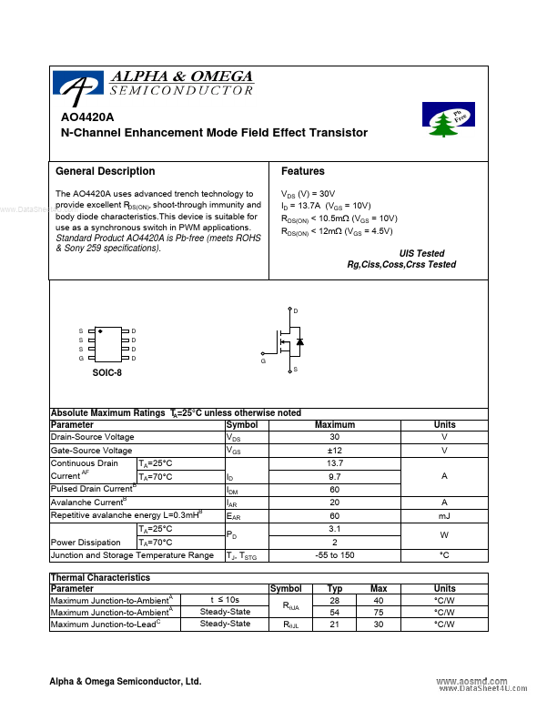
D S S S G D D D D
G S
SOIC-8
Absolute Maximum Ratings T A=25°C unless otherwise noted Parameter Symbol VDS Drain-Source
Voltage VGS Gate-Source
Voltage Continuous Drain TA=25°C Current AF ID TA=70°C Pulsed Drain Current
B B
Maximum 30 ±12 13.7 9.7 60 20 60 3.1 2 -55 to 150
Units V V A A mJ W °C
Avalanche Current Repetitive avalanche energy L=0.3mHB Power Dissipation TA=25°C TA=70°C
IDM IAR EAR PD TJ, TSTG
Junction and Storage Temperature Range Thermal Characteristics Parameter A Maximum Junction-to-Ambient Maximum Junction-to-AmbientA Maximum Junction-to-LeadC
Symbol t ≤ 10s Steady-State Steady-State RθJA RθJL
Typ 28 54 21
Max 40 75 30
Units °C/W °C/W °C/W
Alpha & Omega Semiconductor, Ltd.
www.aosmd.com
AO4420A
Electrical Characteristics (TJ=25°C unless otherwise noted) Parameter Symbol STATIC PARAMETERS BVDSS Drain-Source Breakdown
Voltage IDSS IGSS VGS(th) ID(ON)
www.DataSheet4U.com
Conditions ID=250µA, VGS=0V VDS=24V, VGS=0V TJ=55°C VDS=0V, VGS...