AO4422A N-Channel Enhancement Mode Field Effect Transistor
General Description
The AO4422A uses advanced trench technolo...
AO4422A N-Channel Enhancement Mode Field Effect Transistor
General Description
The AO4422A uses advanced trench technology to provide excellent RDS(ON) and low gate charge. This www.DataSheet4U.com device is suitable for use as a load switch or in PWM applications. The source leads are separated to allow a Kelvin connection to the source, which may be used to bypass the source inductance. Standard Product AO4422A is Pb-free (meets ROHS & Sony 259 specifications). AO4422AL is a Green Product ordering option. AO4422A and AO4422AL are electrically identical.
Features
VDS (V) = 30V ID = 11A (V GS = 10V) RDS(ON) < 15mΩ (VGS = 10V) RDS(ON) < 24mΩ (VGS = 4.5V)
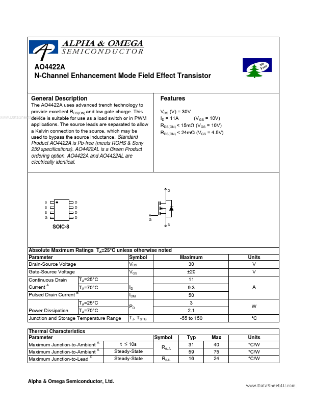
D S S S G D D D D
G S
SOIC-8
Absolute Maximum Ratings TA=25°C unless otherwise noted Parameter Symbol VDS Drain-Source
Voltage VGS Gate-Source
Voltage Continuous Drain Current A Pulsed Drain Current Power Dissipation
B
Maximum 30 ±20 11 9.3 50 3 2.1 -55 to 150
Units V V A
TA=25°C TA=70°C TA=25°C TA=70°C ID IDM PD TJ, TSTG
W °C
Junction and Storage Temperature Range Thermal Characteristics Parameter Maximum Junction-to-Ambient A Maximum Junction-to-Ambient A Maximum Junction-to-Lead C
Symbol t ≤ 10s Steady-State Steady-State RθJA RθJL
Typ 31 59 16
Max 40 75 24
Units °C/W °C/W °C/W
Alpha & Omega Semiconductor, Ltd.
AO4422A
Electrical Characteristics (T J=25°C unless otherwise noted) Parameter Symbol STATIC PARAMETERS BVDSS Drain-Source Breakdown
Voltage IDSS IGSS VGS(th) ID(ON)
www.DataSheet4U.com
Conditions ID...