AO4494
30V N-Channel MOSFET
General Description
The AO4494 combines advanced trench MOSFET technology with a low resist...
AO4494
30V N-Channel
MOSFET
General Description
The AO4494 combines advanced trench
MOSFET technology with a low resistance package to provide extremely low RDS(ON). This device is for PWM applications.
Product Summary
VDS (V) = 30V ID = 18A RDS(ON) < 6.5mΩ RDS(ON) < 9.5mΩ
(VGS = 10V) (VGS = 10V) (VGS = 4.5V)
100% UIS Tested 100% Rg Tested
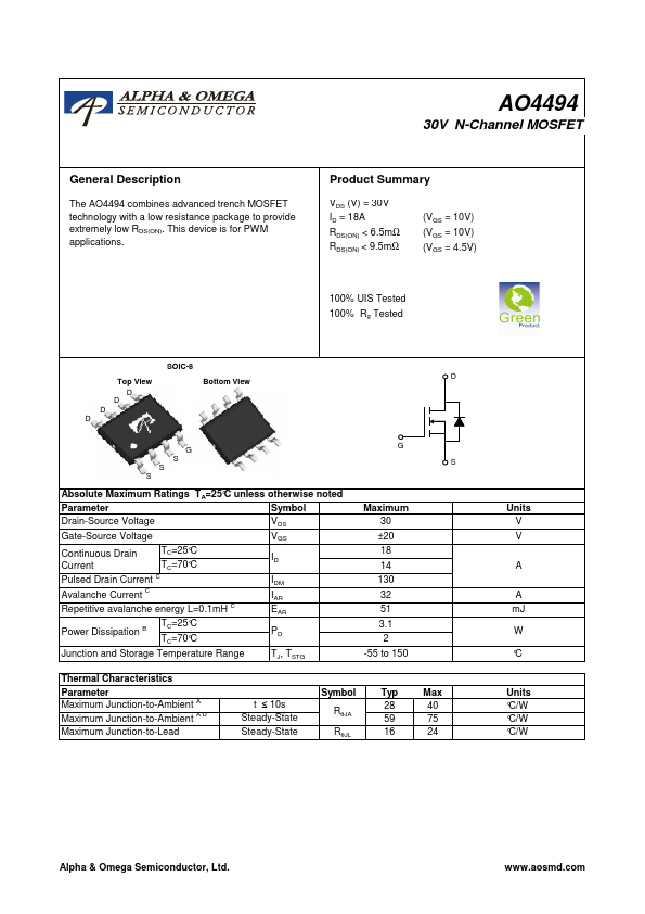
Top View
D D D D
SOIC-8 Bottom View
D
G
S S S
Absolute Maximum Ratings TA=25°C unless otherwise noted
Parameter
Symbol
Drain-Source
Voltage
VDS
Gate-Source
Voltage
VGS
Continuous Drain
TC=25°C
Current
TC=70°C
Pulsed Drain Current C
Avalanche Current C
Repetitive avalanche energy L=0.1mH C
ID
IDM IAR EAR
Power Dissipation B
TC=25°C TC=70°C
PD
Junction and Storage Temperature Range
TJ, TSTG
G
Maximum 30 ±20 18 14 130 32 51 3.1 2
-55 to 150
S
Thermal Characteristics
Parameter Maximum Junction-to-Ambient A Maximum Junction-to-Ambient A D
Maximum Junction-to-Lead
Symbol Typ Max
t ≤ 10s Steady-State
RθJA
28 59
40 75
Steady-State
RθJL 16 24
Units V V
A
A mJ W °C
Units °C/W °C/W °C/W
Alpha & Omega Semiconductor, Ltd.
www.aosmd.com
AO4494
Electrical Characteristics (TJ=25°C unless otherwise noted)
Symbol
Parameter
Conditions
Min Typ Max Units
STATIC PARAMETERS BVDSS Drain-Source Breakdown
Voltage
IDSS Zero Gate
Voltage Drain Current
ID=250µA, VGS=0V VDS=30V, VGS=0V
IGSS VGS(th) ID(ON)
RDS(ON)
gFS VSD IS
Gate-Body leakage current Gate Threshold
Voltage On state drain current
VDS=0V, VGS= ±20V VDS=V...