AO4607 Complementary Enhancement Mode Field Effect Transistor
General Description The AO4607 uses advanced trench techno...
AO4607 Complementary Enhancement Mode Field Effect Transistor
General Description The AO4607 uses advanced trench technology
MOSFETs to provide excellen RDS(ON) and low gate charge. The complementary
MOSFETs may be used in inverter and other applications. A Schottky diode is co-packaged with the nchannel FET to minimize body diode losses. AO4607 is Pb-free (meets ROHS & Sony 259 specifications). AO4607L is a Green Product ordering option. AO4607 and AO4607L are electrically identical.
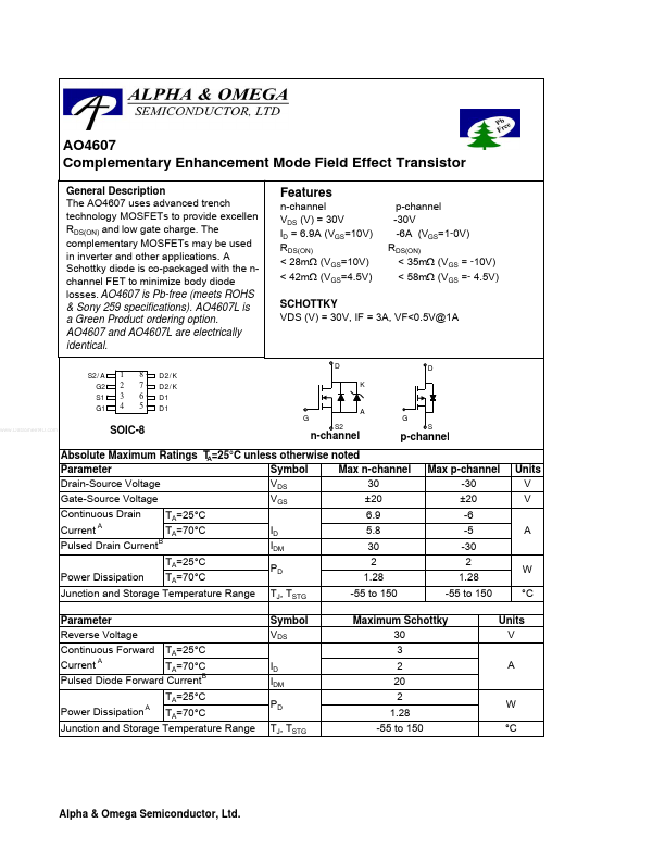
S2/A G2 S1 G1
www.DataSheet4U.com
Features
n-channel VDS (V) = 30V ID = 6.9A (VGS=10V) RDS(ON) < 28mΩ (VGS=10V) < 42mΩ (VGS=4.5V) p-channel -30V -6A (VGS=1-0V) RDS(ON) < 35mΩ (VGS = -10V) < 58mΩ (VGS =- 4.5V)
SCHOTTKY VDS (V) = 30V, IF = 3A, VF<0.5V@1A
1 2 3 4
8 7 6 5
D2/K D2/K D1 D1
D K A S2
D
G
G
SOIC-8
S
n-channel
p-channel Max p-channel -30 ±20 -6 -5 -30 2 1.28 -55 to 150 Units V V A W °C Units V A W °C
Absolute Maximum Ratings T A=25°C unless otherwise noted Parameter Max n-channel Symbol VDS Drain-Source
Voltage 30 VGS Gate-Source
Voltage ±20 Continuous Drain 6.9 TA=25°C A Current TA=70°C 5.8 ID B Pulsed Drain Current IDM 30 TA=25°C TA=70°C Power Dissipation Junction and Storage Temperature Range Parameter Reverse
Voltage Continuous Forward TA=25°C A Current TA=70°C Pulsed Diode Forward CurrentB Power Dissipation
A
PD TJ, TSTG Symbol VDS ID IDM PD TJ, TSTG
2 1.28 -55 to 150
Maximum Schottky 30 3 2 20 2 1.28 -55 to 150
TA=25°C TA=70°C
Junction and Storage Temperature Rang...