AO4614A Complementary Enhancement Mode Field Effect Transistor
General Description
The AO4614A uses advanced trench tec...
AO4614A Complementary Enhancement Mode Field Effect Transistor
General Description
The AO4614A uses advanced trench technology
MOSFETs to provide excellent RDS(ON) and low gate charge. The complementary
MOSFETs may be used in H-bridge, Inverters and other applications. Standard Product AO4614A
is Pb-free (meets ROHS & Sony 259
specifications).
Features
n-channel VDS (V) = 40V ID = 6A (VGS=10V) RDS(ON) < 31mΩ (VGS=10V) < 45mΩ (VGS=4.5V)
p-channel -40V
-5A (VGS = -10V) RDS(ON)
< 45mΩ (VGS = -10V) < 63mΩ (VGS = -4.5V)
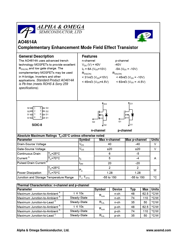
S2 1 8 D2 G2 2 7 D2 S1 3 6 D1 G1 4 5 D1
SOIC-8
D2 D1
G2 S2
G1 S1
n-channel
p-channel
Absolute Maximum Ratings TA=25°C unless otherwise noted
Parameter
Symbol
Max n-channel
Drain-Source
Voltage
VDS 40
Gate-Source
Voltage
VGS ±20
Continuous Drain
TA=25°C
Current A
TA=70°C
Pulsed Drain Current B
ID IDM
6 5 20
Power Dissipation
TA=25°C TA=70°C
PD
2 1.28
Junction and Storage Temperature Range TJ, TSTG
-55 to 150
Max p-channel -40 ±20 -5 -4 -20 2 1.28
-55 to 150
Units V V
A
W °C
Thermal Characteristics: n-channel and p-channel
Parameter
Maximum Junction-to-Ambient A
t ≤ 10s
Maximum Junction-to-Ambient A
Steady-State
Maximum Junction-to-Lead C
Steady-State
Maximum Junction-to-Ambient A
t ≤ 10s
Maximum Junction-to-Ambient A
Steady-State
Maximum Junction-to-Lead C
Steady-State
Symbol RθJA RθJL RθJA RθJL
Device n-ch n-ch n-ch
p-ch p-ch p-ch
Typ Max Units 48 62.5 °C/W 74 110 °C/W 35 50 °C/W
48 62.5 °C/W 74 110 °C/W 35 50 °C/W
...