AOD950A70/AOI950A70
700V, a MOS5 TM N-Channel Power Transistor
General Description
• Proprietary aMOS5TM technology • L...
AOD950A70/AOI950A70
700V, a MOS5 TM N-Channel Power Transistor
General Description
Proprietary aMOS5TM technology Low RDS(ON) Optimized switching parameters for better EMI
performance Enhanced body diode for robustness and fast
reverse recovery
Applications
Flyback for SMPS Charger,Adapter,lighting
Product Summary
VDS @ Tj,max IDM RDS(ON),max Qg,typ Eoss @ 400V
100% UIS Tested 100% Rg Tested
800V 20A < 0.95Ω 9.4nC
1.2mJ
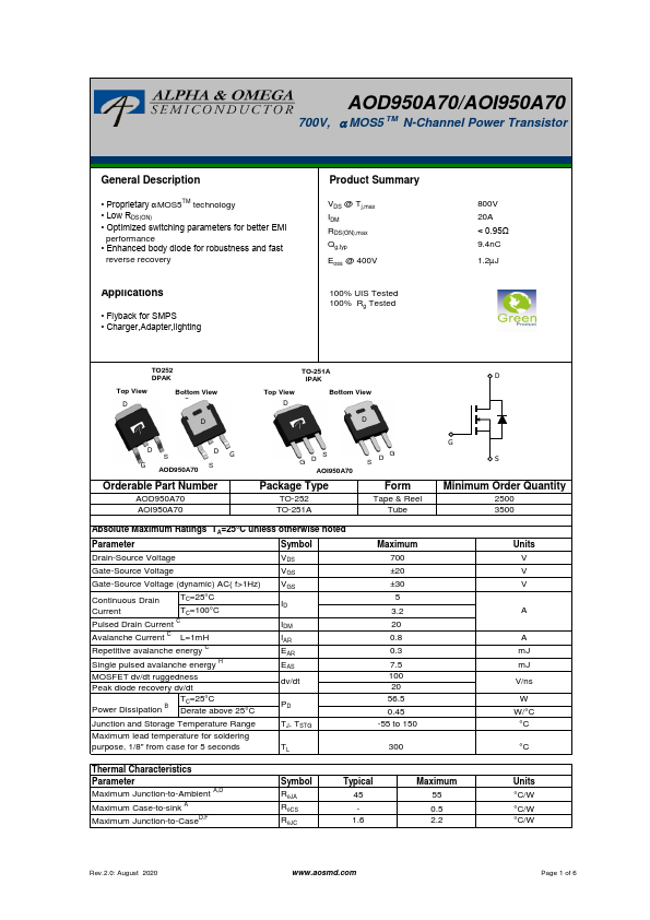
TO252 DPAK
Top View D
Bottom View D
D
S
D S
G AOD950A70
GD
S G
S
Orderable Part Number
AOD950A70 AOI950A70
TO-251A IPAK
Top View D
Bottom View
D
GDS AOI950A70
Package Type
TO-252 TO-251A
S DG
Form
Tape & Reel Tube
D
G S
Minimum Order Quantity
2500 3500
Absolute Maximum Ratings TA=25°C unless otherwise noted
Parameter
Symbol
Drain-Source
Voltage
VDS
Gate-Source
Voltage
Gate-Source
Voltage (dynamic) AC( f>1Hz)
Continuous Drain
TC=25°C
Current
TC=100°C
Pulsed Drain Current C
Avalanche Current C L=1mH
Repetitive avalanche energy C
Single pulsed avalanche energy H
MOSFET dv/dt ruggedness Peak diode recovery dv/dt
VGS VGS
ID
IDM IAR EAR EAS dv/dt
TC=25°C Power Dissipation B Derate above 25°C
PD
Junction and Storage Temperature Range
Maximum lead temperature for soldering purpose, 1/8" from case for 5 seconds
TJ, TSTG TL
Maximum 700 ±20 ±30 5 3.2 20 0.8 0.3 7.5 100 20 56.5 0.45
-55 to 150
300
Units V V V
A
A mJ mJ V/ns W W/°C °C
°C
Thermal Characteristics
Parameter Maximum Junction-to-Ambient A,D Maximum Case-to-...