AONR32314
30V N-Channel MOSFET
General Description
• Latest advanced trench technology • Low RDS(ON) • High Current cap...
AONR32314
30V N-Channel
MOSFET
General Description
Latest advanced trench technology Low RDS(ON) High Current capability RoHS and Halogen-Free Compliant
Applications
Notebook AC-in load switch Battery protection charge/discharge
Product Summary
VDS ID (at VGS=10V) RDS(ON) (at VGS=10V) RDS(ON) (at VGS=4.5V)
100% UIS Tested 100% Rg Tested
30V 30A < 8.7mΩ < 12.3mΩ
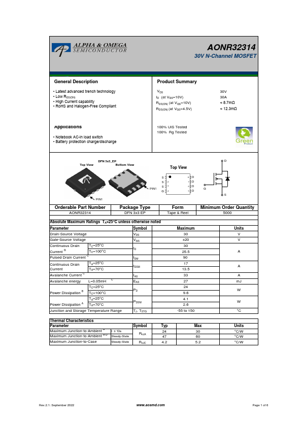
DFN 3x3_EP
D
Top View
Bottom View
Top View
PIN1
Orderable Part Number
AONR32314
PIN1
S1 S2 S3 G4
8D 7D 6D
G 5D
S
Package Type
DFN 3x3 EP
Form
Tape & Reel
Minimum Order Quantity
5000
Absolute Maximum Ratings TA=25°C unless otherwise noted
Parameter
Symbol
Drain-Source
Voltage
VDS
Gate-Source
Voltage
VGS
Continuous Drain Current G
TC=25°C TC=100°C
ID
Pulsed Drain Current C
IDM
Continuous Drain Current
TA=25°C TA=70°C
IDSM
Avalanche Current C
IAS
Avalanche energy L=0.05mH C
EAS
TC=25°C Power Dissipation B TC=100°C
PD
TA=25°C Power Dissipation A TA=70°C
PDSM
Junction and Storage Temperature Range
TJ, TSTG
Maximum 30 ±20 30 25.5 90 17 13.5 33 27 24 9.6 4.1 2.6
-55 to 150
Units V V
A
A A mJ W
W °C
Thermal Characteristics
Parameter
Symbol
Typ
Maximum Junction-to-Ambient A t ≤ 10s
Maximum Junction-to-Ambient A D Steady-State
RqJA
24 47
Maximum Junction-to-Case
Steady-State
RqJC
4.2
Max 30 60 5.2
Units °C/W °C/W °C/W
Rev.2.1: September 2022
www.aosmd.com
Page 1 of 6
AONR32314
Electrical Characteristics (TJ=25°C unless otherwise noted)
Symbol Parameter
Co...