AONV210A60
600V, a MOS5 TM N-Channel Power Transistor
General Description
• Proprietary aMOS5TM technology • Low RDS(ON...
AONV210A60
600V, a MOS5 TM N-Channel Power Transistor
General Description
Proprietary aMOS5TM technology Low RDS(ON) Optimized switching parameters for better EMI
performance Enhanced body diode for robustness and fast reverse
recovery
Applications
SMPS with PFC,Flyback and LLC topologies Silver ATX,adapter,TV,lighting, Telecom
Product Summary
VDS @ Tj,max IDM RDS(ON),max Qg,typ Eoss @ 400V
100% UIS Tested 100% Rg Tested
700V 80A < 0.21Ω 34nC
4.3mJ
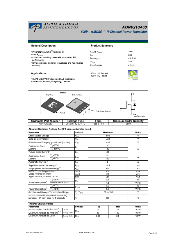
Top View
DFN8X8
Bottom View
D
D
Pin1:G
S
S
Orderable Part Number
AONV210A60
Package Type
DFN8x8_4L_EP1_S
G
Pin2: Driver Source
G
S Driver Source
Form
Tape & Reel
Minimum Order Quantity
3500
Absolute Maximum Ratings TA=25°C unless otherwise noted
Parameter
Symbol
Drain-Source
Voltage
VDS
Gate-Source
Voltage
VGS
Gate-Source
Voltage (dynamic) AC( f>1Hz)
Continuous Drain
TC=25°C
Current
TC=100°C
Pulsed Drain Current C
Continuous Drain Current Avalanche Current C
TA=25°C TA=70°C
Repetitive avalanche energy C
Single pulsed avalanche energy G
MOSFET dv/dt ruggedness
Diode reverse recovery VDS=0 to 400V,IF<=20A,Tj=25°C
VGS
ID
IDM
IDSM
IAR EAR EAS dv/dt dv/dt di/dt
TC=25°C Power Dissipation B Derate above 25°C
PD
TA=25°C Power Dissipation A TA=70°C
PDSM
Junction and Storage Temperature Range
Maximum lead temperature for soldering purpose, 1/8" from case for 5 seconds
TJ, TSTG TL
Maximum 600 ±20 ±30 20 12 80 4.1 3.3 5 12.5 410 100 20 250 208 1.6 8.3 5.3
-55 to 150
300
Units V V V
A
A
...