AONY36356
30V Dual Asymmetric N-Channel MOSFET
General Description
• Trench Power MOSFET technology • Low RDS(ON) at 4....
AONY36356
30V Dual Asymmetric N-Channel
MOSFET
General Description
Trench Power
MOSFET technology Low RDS(ON) at 4.5V Vgs Low Gate Charge High Current Capability RoHS and Halogen-Free Compliant
Applications
DC/DC Converters in Computer See Note I
Product Summary
VDS ID (at VGS=10V) RDS(ON) (at VGS=10V) RDS(ON) (at VGS=4.5V)
Q1 Q2 30V 30V
32A 32A < 6.1mΩ < 3.8mΩ < 9.6mΩ < 4.7mΩ
100% UIS Tested 100% Rg Tested
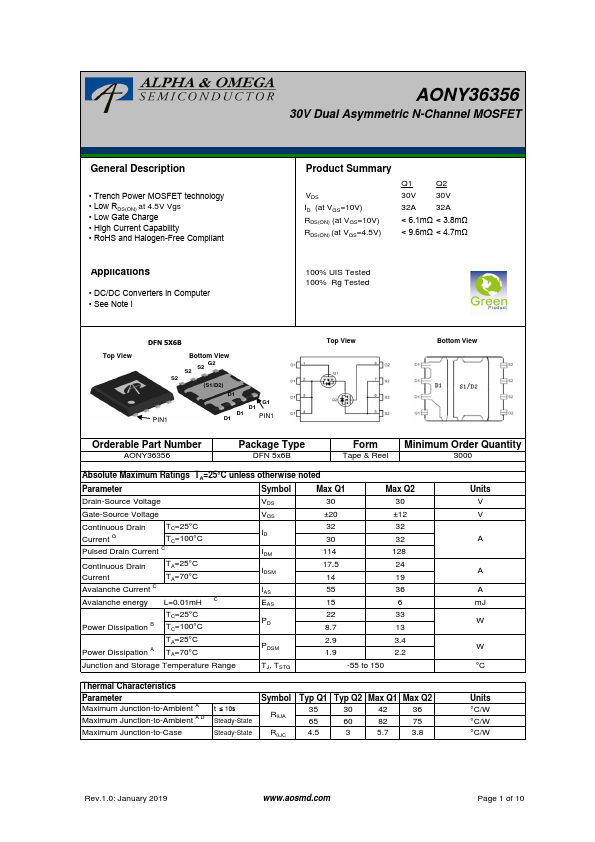
Top View
DFN 5X6B
S2 PIN1
Bottom View S2 G2
S2
(S1/D2)
D1
G1
D1
D1 D1
PIN1
Top View
Bottom View
Orderable Part Number
AONY36356
Package Type
DFN 5x6B
Form
Minimum Order Quantity
Tape & Reel
3000
Absolute Maximum Ratings TA=25°C unless otherwise noted
Parameter
Symbol
Max Q1
Max Q2
Drain-Source
Voltage
VDS 30
30
Gate-Source
Voltage
Continuous Drain TC=25°C
Current G
TC=100°C
Pulsed Drain Current C
Continuous Drain Current Avalanche Current C
TA=25°C TA=70°C
Avalanche energy L=0.01mH
TC=25°C Power Dissipation B TC=100°C
C
VGS ID
IDM IDSM
IAS EAS PD
±20 32 30 114 17.5 14 55 15 22 8.7
±12 32 32 128 24 19 36 6 33 13
TA=25°C Power Dissipation A TA=70°C
PDSM
2.9 1.9
3.4 2.2
Junction and Storage Temperature Range
TJ, TSTG
-55 to 150
Units V V
A
A A mJ W
W °C
Thermal Characteristics
Parameter Maximum Junction-to-Ambient A Maximum Junction-to-Ambient A D
Maximum Junction-to-Case
t ≤ 10s Steady-State Steady-State
Symbol RqJA RqJC
Typ Q1 Typ Q2 Max Q1 Max Q2 35 30 42 36 65 60 82 75 4.5 3 5.7 3.8
Units °C/W °C/W °C/W...