www.DataSheet4U.com
AOU400 N-Channel Enhancement Mode Field Effect Transistor
General Description
The AOU400 uses advan...
www.DataSheet4U.com
AOU400 N-Channel Enhancement Mode Field Effect Transistor
General Description
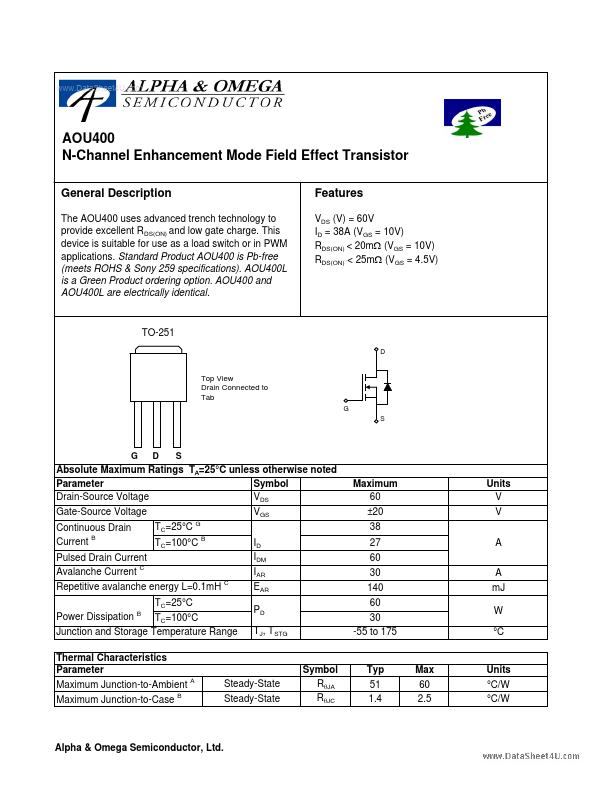
The AOU400 uses advanced trench technology to provide excellent RDS(ON) and low gate charge. This device is suitable for use as a load switch or in PWM applications. Standard Product AOU400 is Pb-free (meets ROHS & Sony 259 specifications). AOU400L is a Green Product ordering option. AOU400 and AOU400L are electrically identical.
Features
VDS (V) = 60V ID = 38A (VGS = 10V) RDS(ON) < 20mΩ (VGS = 10V) RDS(ON) < 25mΩ (VGS = 4.5V)
TO-251
D Top View Drain Connected to Tab G S
G
D
S
Absolute Maximum Ratings TA=25°C unless otherwise noted Symbol Parameter VDS Drain-Source
Voltage VGS Gate-Source
Voltage Continuous Drain Current B Pulsed Drain Current Avalanche Current C Repetitive avalanche energy L=0.1mH C TC=25°C Power Dissipation TC=100°C Junction and Storage Temperature Range Thermal Characteristics Parameter Maximum Junction-to-Ambient Maximum Junction-to-Case B
A B
Maximum 60 ±20 38 27 60 30 140 60 30 -55 to 175
Units V V A A mJ W °C
TC=25°C
G B
TC=100°C
ID IDM IAR EAR PD TJ, TSTG
Steady-State Steady-State
Symbol RθJA RθJC
Typ 51 1.4
Max 60 2.5
Units °C/W °C/W
Alpha & Omega Semiconductor, Ltd.
AOU400
www.DataSheet4U.com Electrical Characteristics (TJ=25°C unless otherwise noted)
Symbol
Parameter
Conditions ID=250µA, VGS=0V VDS=48V, VGS=0V TJ=55°C VDS=0V, VGS= ±20V VDS=VGS ID=250µA VGS=10V, VDS=5V VGS=10V, ID=20A TJ=125°C VGS=4.5V, ID=20A VDS=5V, ID=20A
Min...