AP1003BST
Preliminary
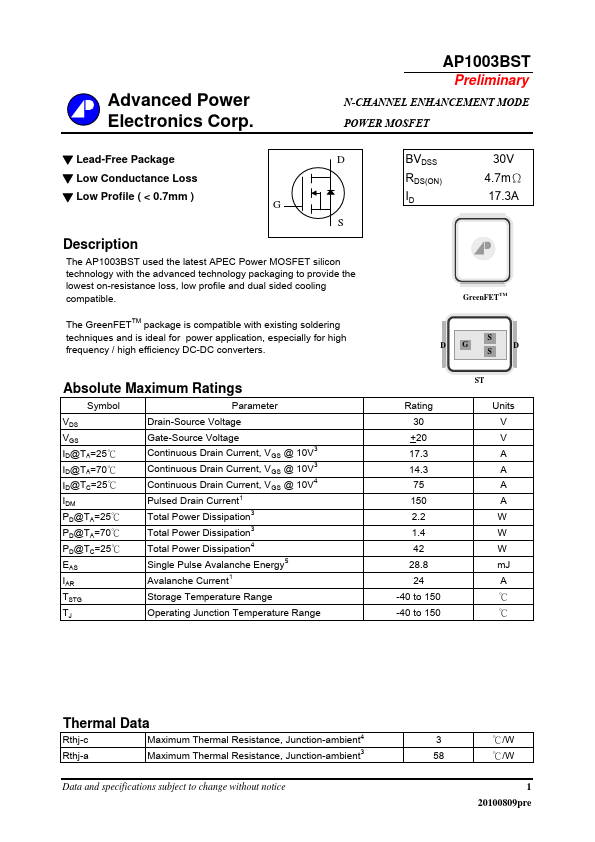
Advanced Power Electronics Corp.
▼ Lead-Free Package ▼ Low Conductance Loss ▼ Low Profile ( < 0.7...
AP1003BST
Preliminary
Advanced Power Electronics Corp.
▼ Lead-Free Package ▼ Low Conductance Loss ▼ Low Profile ( < 0.7mm ) G S
N-CHANNEL ENHANCEMENT MODE POWER
MOSFET D
BVDSS RDS(ON) ID
30V 4.7mΩ 17.3A
Description
The AP1003BST used the latest APEC Power
MOSFET silicon technology with the advanced technology packaging to provide the lowest on-resistance loss, low profile and dual sided cooling compatible. The GreenFETTM package is compatible with existing soldering techniques and is ideal for power application, especially for high frequency / high efficiency DC-DC converters.
GreenFETTM
D
G
S S D
Absolute Maximum Ratings
Symbol VDS VGS ID@TA=25℃ ID@TA=70℃ ID@TC=25℃ IDM PD@TA=25℃ PD@TA=70℃ PD@TC=25℃ EAS IAR TSTG TJ Parameter Drain-Source
Voltage Gate-Source
Voltage Continuous Drain Current, V GS @ 10V Continuous Drain Current, V GS @ 10V Continuous Drain Current, V GS @ 10V Pulsed Drain Current
1 3 3 4 5 3 3 4
ST
Rating 30 +20 17.3 14.3 75 150 2.2 1.4 42 28.8 24 -40 to 150 -40 to 150
Units V V A A A A W W W mJ A ℃ ℃
Total Power Dissipation Total Power Dissipation Total Power Dissipation Avalanche Current
1
Single Pulse Avalanche Energy Storage Temperature Range
Operating Junction Temperature Range
Thermal Data
Rthj-c Rthj-a Maximum Thermal Resistance, Junction-ambient4 Maximum Thermal Resistance, Junction-ambient
3
3 58
℃/W ℃/W 1 20100809pre
Data and specifications subject to change without notice
AP1003BST
Electrical Characteristics@Tj=25oC(unless otherw...