AP3403GH/J
Pb Free Plating Product
Advanced Power Electronics Corp.
▼ Low Gate Charge ▼ Simple Drive Requirement ▼ Fast...
AP3403GH/J
Pb Free Plating Product
Advanced Power Electronics Corp.
▼ Low Gate Charge ▼ Simple Drive Requirement ▼ Fast Switching G S D
P-CHANNEL ENHANCEMENT MODE POWER
MOSFET
BVDSS RDS(ON) ID
-30V 200mΩ - 10A
Description
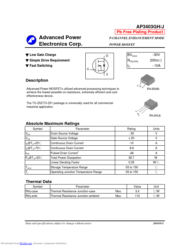
G D
Advanced Power
MOSFETs utilized advanced processing techniques to achieve the lowest possible on-resistance, extremely efficient and costeffectiveness device. The TO-252/TO-251 package is universally used for all commercialindustrial application.
G D S
S
TO-252(H)
TO-251(J)
Absolute Maximum Ratings
Symbol VDS VGS ID@TA=25℃ ID@TA=70℃ IDM PD@TA=25℃ TSTG TJ Parameter Drain-Source
Voltage Gate-Source
Voltage Continuous Drain Current Continuous Drain Current Pulsed Drain Current
1
Rating - 30 ± 20 -10 -8.6 -48 36.7 0.29 -55 to 150 -55 to 150
Units V V A A A W W/ ℃ ℃ ℃
Total Power Dissipation Linear Derating Factor Storage Temperature Range Operating Junction Temperature Range
Thermal Data
Symbol Rthj-case Rthj-amb Parameter Thermal Resistance Junction-case Thermal Resistance Junction-ambient Max. Max. Value 3.4 110 Unit ℃/W ℃/W
Data and specifications subject to change without notice
200505031
Downloaded from Elcodis.com electronic components distributor
AP3403GH/J
Electrical Characteristics@Tj=25oC(unless otherwise specified)
Symbol BVDSS
ΔBVDSS/ΔTj
Parameter Drain-Source Breakdown
Voltage
2
Test Conditions VGS=0V, ID=-250uA
Min. -30 -1 -
Typ. -0.1
Max. Units 200 400 -3 -1 -25 ±100 V V/℃ mΩ mΩ V S uA uA nA nC nC nC ns ns ns ns pF pF pF...