www.DataSheet4U.com
AP4501GD
Pb Free Plating Product
Advanced Power Electronics Corp.
▼ Low Gate Charge ▼ Fast Switchi...
www.DataSheet4U.com
AP4501GD
Pb Free Plating Product
Advanced Power Electronics Corp.
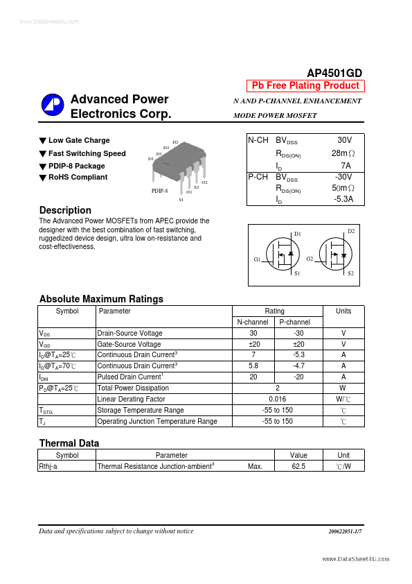
▼ Low Gate Charge ▼ Fast Switching Speed ▼ PDIP-8 Package ▼ RoHS Compliant
PDIP-8
S1 S2 G1 D2 D1 D1 D2
N AND P-CHANNEL ENHANCEMENT MODE POWER
MOSFET
N-CH BVDSS RDS(ON) ID P-CH BVDSS RDS(ON) ID
30V 28mΩ 7A -30V 5 0m Ω -5.3A
G2
Description
The Advanced Power
MOSFETs from APEC provide the designer with the best combination of fast switching, ruggedized device design, ultra low on-resistance and cost-effectiveness.
G1 S1 D1 D2
G2 S2
Absolute Maximum Ratings
Symbol VDS VGS ID@TA=25℃ ID@TA=70℃ IDM PD@TA=25℃ TSTG TJ Parameter Drain-Source
Voltage Gate-Source
Voltage Continuous Drain Current 3 Continuous Drain Current Pulsed Drain Current
1 3
Rating N-channel 30 ±20 7 5.8 20 2 0.016 -55 to 150 -55 to 150 P-channel -30 ±20 -5.3 -4.7 -20
Units V V A A A W W/ ℃ ℃ ℃
Total Power Dissipation Linear Derating Factor Storage Temperature Range Operating Junction Temperature Range
Thermal Data
Symbol Rthj-a Parameter Thermal Resistance Junction-ambient
3
Value Max. 62.5
Unit ℃/W
Data and specifications subject to change without notice
200622051-1/7
www.DataSheet4U.com
AP4501GD
N-CH Electrical Characteristics@Tj=25 C(unless otherwise specified)
Symbol BVDSS ΔBVDSS/ΔTj RDS(ON) VGS(th) gfs IDSS IGSS Qg Qgs Qgd td(on) tr td(off) tf Ciss Coss Crss Rg Parameter Drain-Source Breakdown
Voltage Test Conditions VGS=0V, ID=250uA Min. 30 1 Typ. 0.02 13 9 2 5 6 5 19 5 645 150 95 1.6 Max. Units 28 42 3 1 ...