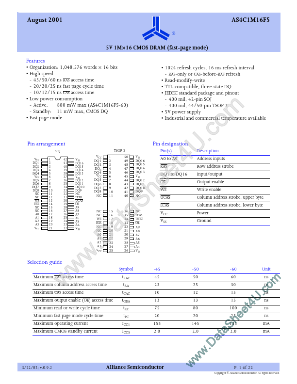
August 2001
®
AS4C1M16F5
5V 1M×16 CMOS DRAM (fast-page mode) Features
• Organization: 1,048,576 words × 16 bits • High...
August 2001
®
AS4C1M16F5
5V 1M×16
CMOS DRAM (fast-page mode) Features
Organization: 1,048,576 words × 16 bits High speed - 45/50/60 ns RAS access time - 20/20/25 ns fast page cycle time - 10/12/15 ns CAS access time Low power consumption - Active: 880 mW max (AS4C1M16F5-60) - Standby: 11 mW max,
CMOS DQ Fast page mode 1024 refresh cycles, 16 ms refresh interval - RAS-only or CAS-before-RAS refresh Read-modify-write TTL-compatible, three-state DQ JEDEC standard package and pinout - 400 mil, 42-pin SOJ - 400 mil, 44/50-pin TSOP 2 5V power supply Industrial and commercial temperature available
Pin arrangement
SOJ
Vcc DQ1 DQ2 DQ3 '4 Vcc DQ5 DQ6 1 2 3 4 5 6 7 8 9 10 11 12 13 14 15 16 17 18 19 20 21
DQ7
DQ8 NC NC WE RAS NC NC A0 A1
A2
A3 Vcc
Selection guide
Maximum RAS access time Maximum CAS access time
Maximum column address access time
m o .c U 4 t e e h S a t a .D w w w
Pin designation
Pin(s)
RAS
TSOP 2
Description
42 41 40 39 38 37 36 35 34 33 32 31 30 29 28 27 26 25 24 23 22
VSS
DQ16 DQ15 DQ14 DQ13
VSS
DQ12 DQ11
DQ10
DQ9 NC LCAS UCAS OE A9 A8 A7 A6 A5
VCC DQ1 DQ2 DQ3 DQ4 VCC DQ5 DQ6 DQ7 DQ8 NC
1 2 3 4 5 6 7 8 9 10 11
50 49 48 47 46 45 44 43 42 41 40
VSS DQ16 DQ15 DQ14 DQ13 VSS DQ12 DQ11 DQ10 DQ9 NC
A0 to A9
Address inputs Input/output
Row address strobe Output enable Write enable
DQ1 to DQ16
OE
WE
UCAS LCAS
Column address strobe, upper byte Column address strobe, lower byte Power Ground
NC NC
A4 VSS
WE RAS
NC NC A0 A1 A2 A...