B9940L
2.5V or 3.3V, 200-MHz, 1:18 Clock Distribution Buffer
Features
• • • • • • 200-MHz clock support LVPECL or LVCMO...
B9940L
2.5V or 3.3V, 200-MHz, 1:18 Clock Distribution Buffer
Features
200-MHz clock support LVPECL or LV
CMOS/LVTTL clock input LV
CMOS/LVTTL compatible inputs 18 clock outputs: drive up to 36 clock lines 150-ps max. output-to-output skew Dual- or single-supply operation: — 3.3V core and 3.3V outputs — 3.3V core and 2.5V outputs — 2.5V core and 2.5V outputs Pin-compatible with MPC940L Industrial temperature range: -40°C to 85°C 32-pin LQFP package
Description
The B9940L is a low-
voltage clock distribution buffer with the capability to select either a differential LVPECL- or an LV
CMOS/LVTTL-compatible input clock. The two clock sources can be used to provide for a test clock as well as the primary system clock. All other control inputs are LV
CMOS/LVTTL compatible. The eighteen outputs are 2.5V or 3.3V compatible and can drive two series-terminated 50Ω transmission lines. With this capability the B9940L has an effective fan-out of 1:36. Low output-to-output skews make the B9940L an ideal clock distribution buffer for nested clock trees in the most demanding of synchronous systems.
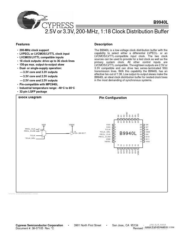
Block Diagram
Pin Configuration
VDDC
32
31
30
29
28
27
26
25
VSS
Q0
Q1
Q2
Q3
Q4
Q5
VDD PECL_CLK PECL_CLK# TCLK TCLK_SEL 0 1
VDDC
18
Q0-Q17
VSS VSS TCLK T C LK _S E L P E C L _C L K P E C L_ C LK # VDD VDDC
1 2 3 4 5 6 7 8 9
B9940L
10 11 12 13 14 15 16
24 23 22 21 20 19 18 17
Q6 Q7 Q8 VDD Q9 Q 10 Q 11 VSS
Q17
Q16
Q15
Q14
Q13
VSS
Q12
www.DataSheet4U.c...