B9949
3.3V 160-MHz 1:15 Clock Distribution Buffer
Features
• • • • • • • • • • 160MHz Clock Support LVPECL or LVCMOS/LV...
B9949
3.3V 160-MHz 1:15 Clock Distribution Buffer
Features
160MHz Clock Support LVPECL or LV
CMOS/LVTTL Clock Input LV
CMOS/LVTTL Compatible Inputs 15 Clock Outputs: Drive up to 30 Clock Lines 1X and 1/2X Configurable Outputs Output Three-state Control 350 ps Maximum Output-to-Output Skew Pin Compatible with MPC949 Industrial Temp. Range: –40°C to +85°C 52-Pin TQFP Package
Description
The B9949 is a low-
voltage clock distribution buffer with the capability to select either a differential LVPECL or LV
CMOS/LVTTL compatible input clocks. These clock sources can be used to provide for test clocks as well as the primary system clocks. All other control inputs are LV
CMOS/LVTTL compatible. The 15 outputs are 3.3V LV
CMOS or LVTTL compatible and can drive two series terminated 50Ω transmission lines. With this capability the B9949 has an effective fan-out of 1:30. The B9949 is capable of generating 1X and 1/2X signals from a 1X source. These signals are generated and retimed internally to ensure minimal skew between the 1X and 1/2X signals. SEL(A:D) inputs allow flexibility in selecting the ratio of 1X to1/2X outputs. The B9949 outputs can also be three-stated via MR/OE# input. When MR/OE# is set HIGH, it resets the internal flip-flops and three-states the outputs.
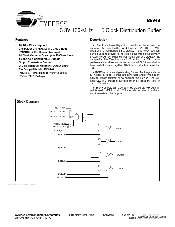
Block Diagram
TCLK_SEL TCLK0 (LVTTL) TCLK1 (LVTTL) PECL_CLK PECL_CLK# PCLK_SEL DSELA
0 1
0 0 1 1 /2 R 0 1 /1
2
QA0:1
3
QB0:2
DSELB
0 1
4
QC0:3
DSELC
0 1
6
QD0:5
DSELD MR/OE#
www.DataSheet4U...