BCR101...
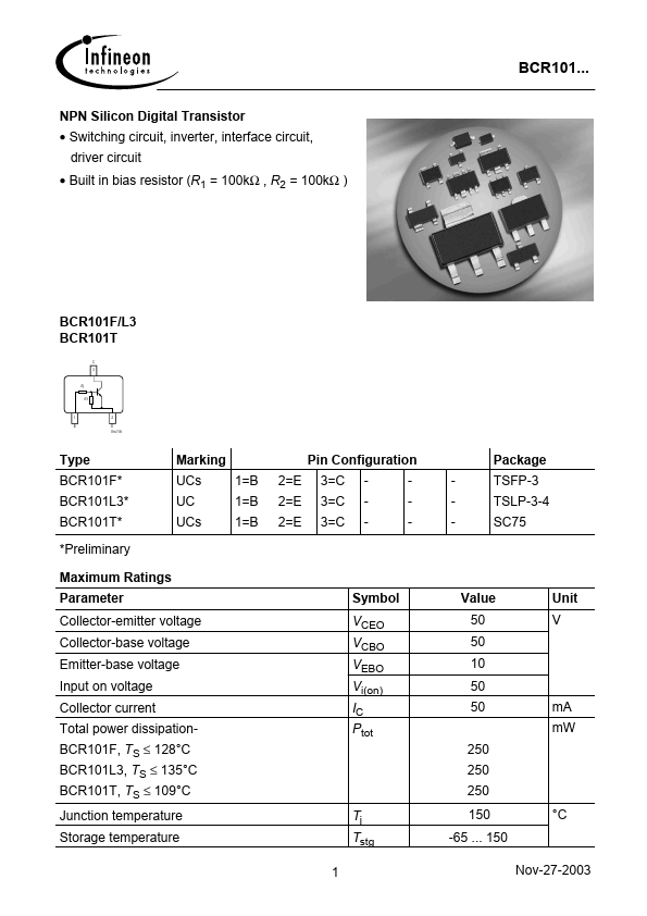
NPN Silicon Digital Transistor • Switching circuit, inverter, interface circuit, driver circuit • Built in bia...
BCR101...
NPN Silicon Digital Transistor Switching circuit, inverter, interface circuit, driver circuit Built in bias resistor (R1 = 100kΩ , R2 = 100kΩ )
BCR101F/L3 BCR101T
C 3
R1 R2
1 B
2 E
EHA07184
Type
Marking
Pin Configuration
Package
BCR101F* BCR101L3* BCR101T* *Preliminary
Maximum Ratings Parameter
UCs UC UCs
1=B 1=B 1=B
2=E 2=E 2=E
3=C 3=C 3=C
-
-
-
TSFP-3 TSLP-3-4 SC75
Symbol VCEO VCBO VEBO Vi(on) IC Ptot
Value 50 50 10 50 50 250 250 250
Unit V
Collector-emitter
voltage Collector-base
voltage Emitter-base
voltage Input on
voltage Collector current Total power dissipationBCR101F, TS ≤ 128°C BCR101L3, TS ≤ 135°C BCR101T, TS ≤ 109°C Junction temperature Storage temperature
1
mA mW
Tj Tstg
150 -65 ... 150
°C
Nov-27-2003
BCR101...
Thermal Resistance Parameter Junction - soldering point1) BCR101F BCR101L3 BCR101T Symbol RthJS Value
≤ 90 ≤ 60 ≤ 165
Unit K/W
Electrical Characteristics at TA = 25°C, unless otherwise specified Symbol Values Unit Parameter min. typ. max. DC Characteristics Collector-emitter breakdown
voltage V(BR)CEO 50 V
IC = 100 µA, IB = 0
Collector-base breakdown
voltage
IC = 10 µA, IE = 0
V(BR)CBO I CBO I EBO h FE VCEsat Vi(off) Vi(on) R1 R1/R 2
50 70 0.5 1 70 0.9
-
100 1
100 3
100 75 0.3 1.8 3 130 1.1
kΩ
Collector-base cutoff current
VCB = 40 V, IE = 0
nA µA V
Emitter-base cutoff current
VEB = 10 V, IC = 0
DC current gain2)
IC = 5 mA, VCE = 5 V
Collector-emitter saturation
voltage2)
IC = 5 mA, IB = 0.25 mA
Input o...