BFW10 – BFW11
N CHANNEL SILICON FETS
DESCRIPTION :
Symmetrical N-CHANNEL silicon planar epitaxial junction field-effect ...
BFW10 – BFW11
N CHANNEL SILICON FETS
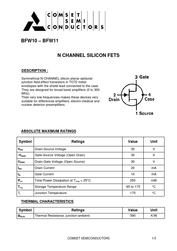
DESCRIPTION :
Symmetrical N-CHANNEL silicon planar epitaxial junction field-effect transistors in TO72 metal envelopes with the shield lead connected to the case. They are designed for broad band
amplifiers (0 to 300 MHz). Their very low frequencies makes these devices very suitable for differencial
amplifiers, electro-medical and nuclear detector pre
amplifiers.
ABSOLUTE MAXIMUM RATINGS
Symbol
Ratings
VDS -VGSO VDGO IDS IG Ptot Tstg Tj
Drain-Source
Voltage Gate-Source
Voltage (Open Drain) Drain-Gate
Voltage (Open Source) Drain Current Gate Current Total Power Dissipation at Tamb = 25°C Storage Temperature Range Junction Temperature
THERMAL CHARACTERISTICS
Symbol
Ratings
RthJA
Thermal Resistance, junction-ambient
Value
30 30 30 20 10 250 -65 to 175 175
Unit
V V V mA mA mW °C °C
Value
590
Unit
K/W
19/08/2014
COMSET SEMICONDUCTORS
1/3
BFW10 – BFW11
ELECTRICAL CHARACTERISTICS Tj = 25°C unless otherwise specified
Symbol
Ratings
-IGSS
Gate Cutoff Current
IDSS Drain Current
-VGS
Gate Source
Voltage
-V(P)GS
Gate Source Cutoff
Voltage
Test Condition(s)
-VGS = 20V VDS = 0
-VGS = 20V ; VDS = 0 Tj = 150°C
BFW10 BFW11 BFW10
BFW11
VDS = 15V VGS = 0
BFW10 BFW11
ID= 400µA BFW10 VDS = 15V
ID= 50µA BFW11
VDS = 15V ID= 0.5nA
BFW10 BFW11
Min Typ Max Unit
- - 0.1 nA
-
8 4 2 1.25 -
-
-
0.5 µA
20 mA
10
7.5 V
4
8 V
6
SMALL SIGNAL CHARACTERISTICS
Tj = 25°C unless otherwise specified
Symbol
Ratings
Test Condition(s)
VDS ...