6A,650V N-Channel Power Mosfet
FEATURES
RDS(ON) =1.7Ω@ VGS = 10V Ultra low gate charge ( typical 20 nC )
Pb
Lead-...
6A,650V N-Channel Power
Mosfet
FEATURES
RDS(ON) =1.7Ω@ VGS = 10V Ultra low gate charge ( typical 20 nC )
Pb
Lead-free
Low reverse transfer Capacitance ( CRSS = typical 10 pF )
Fast switching capability
Avalanche energy specified
Improved dv/dt capability, high ruggedness
Production specification
BL6N65I/BL6N65D
MAXIMUM RATING @ Ta=25℃ unless otherwise specified
Symbol
Parameter
VDSS
Drain-Source
voltage
VGSS
ID
IDM EAS EAR dv/dt
Gate -Source
voltage
Continuous Drain Current
Pulsed Drain Current
Avalanche Energy
Single Pulsed Repetitive
Peak Diode Recovery dv/dt
PD Power Dissipation RθJA Thermal resistance,Junction-to-Ambient
TJ Junction Temperature
TOPR, Tstg Operating and Storage Temperature
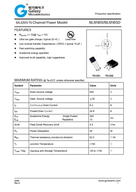
TO-251 TO-252
Value 650
±30 6.2 24.8 440 13 4.5 40 62.5
+150
-55 to +150
Units V V A A mJ V/ns W ℃/W ℃ ℃
S066 Rev.A
www.gmesemi.com
1
Production specification
6A,650V N-Channel Power
Mosfet
BL6N65I/BL6N65D
ELECTRICAL CHARACTERISTI...