Multilayer Chip Beads
Advantages of using Multi Layer Chips Features
1. 2. 3. 4. 5. 6. Small size chips generate high im...
Multilayer Chip Beads
Advantages of using Multi Layer Chips Features
1. 2. 3. 4. 5. 6. Small size chips generate high impedance. Minimum floating capacity and excellent high frequency characteristics. Outstanding soldering heat resistance. Both flow and reflow soldering methods can be used. Perfect shape for automatic mounting, with no directionality. Monolithic inorganic material construction for high reliability. Closed magnetic circuit avoids crosstalk and is suited to high density printed circuit boards.
Common Applications for Impedance Chips
Clock generation circuitry, filtering between analogue and digital circuitry, I/O interconnectors (e.g. serial, parallel, keyboard, mouse, telecommunications, local area networks), isolation between RF noisy circuits and logic circuits and logic devices susceptible to functional degradation, power supply filtering to prevent conducted RF energy from corrupting the power generation circuitry, high frequency EMI prevention of computers, VCR's, TV's and portable telephones.
About using Multi Layer Chips
Chip Beads (Impeders), perform the function of removing RF energy that exists within a transmission line structure (Printed circuit board tracking). This RF energy is an AC sine wave component that co-exists with the DC
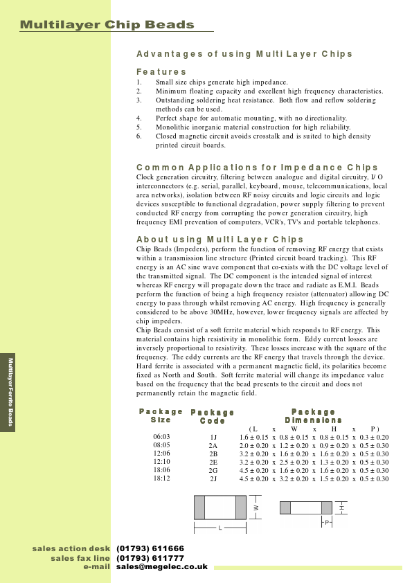
voltage level of the transmitted signal. The DC component is the intended signal of interest whereas RF energy will propagate down the trace and radiate as E.M.I. Beads perform the function of being a high frequency re...