BS170G
Small Signal MOSFET 500 mA, 60 Volts
N−Channel TO−92 (TO−226)
Features
• This is a Pb−Free Device*
MAXIMUM RAT...
BS170G
Small Signal
MOSFET 500 mA, 60 Volts
N−Channel TO−92 (TO−226)
Features
This is a Pb−Free Device*
MAXIMUM RATINGS
Rating
Symbol Value Unit
Drain −Source
Voltage
Gate−Source
Voltage − Continuous − Non−repetitive (tp ≤ 50 ms)
Drain Current (Note)
Total Device Dissipation @ TA = 25°C
Operating and Storage Junction Temperature Range
VDS 60
VGS VGSM
ID PD TJ, Tstg
± 20 ± 40
0.5
350
−55 to +150
Vdc
Vdc Vpk Adc mW °C
Stresses exceeding Maximum Ratings may damage the device. Maximum Ratings are stress ratings only. Functional operation above the Recommended Operating Conditions is not implied. Extended exposure to stresses above the Recommended Operating Conditions may affect device reliability.
NOTE: The Power Dissipation of the package may result in a lower continuous drain current.
http://onsemi.com
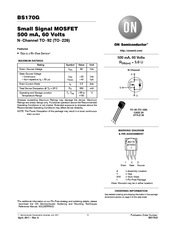
500 mA, 60 Volts RDS(on) = 5.0 W
N−Channel D
G
S
123
TO−92 (TO−226) CASE 29 STYLE 30
MARKING DIAGRAM & PIN ASSIGNMENT
BS170 AYWWG
G
*For additional information on our Pb−Free strategy and soldering details, please download the ON Semiconductor Soldering and Mounting Techniques Reference Manual, SOLDERRM/D.
© Semiconductor Components Industries, LLC, 2011
April, 2011 − Rev. 6
1
123 Drain Gate Source A = Assembly Location Y = Year WW = Work Week G = Pb−Free Package (Note: Microdot may be in either location)
ORDERING INFORMATION
See detailed ordering and shipping information in the package dimensions section on page 2 of this data sheet.
Publication Order Numbe...