BS807
N-CHANNEL ENHANCEMENT MODE DMOS TRANSISTOR Features
· · · · · High Breakdown Voltage High Input Impedance Fast Swi...
BS807
N-CHANNEL ENHANCEMENT MODE DMOS TRANSISTOR Features
· · · · · High Breakdown
Voltage High Input Impedance Fast Switching Speed Specially Suited for Telephone Subsets Ideal for Automated Surface Mount Assembly
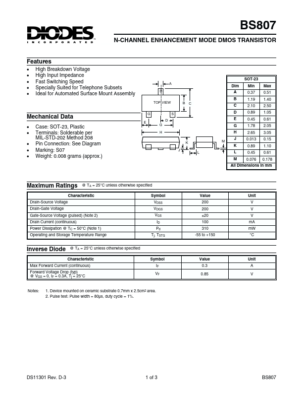
SOT-23
A D TOP VIEW G E D G H K J L M S B C
Dim A B C D E G H J K L M
Min 0.37 1.19 2.10 0.89 0.45 1.78 2.65 0.013 0.89 0.45 0.076
Max 0.51 1.40 2.50 1.05 0.61 2.05 3.05 0.15 1.10 0.61 0.178
Mechanical Data
· · · · · Case: SOT-23, Plastic Terminals: Solderable per MIL-STD-202 Method 208 Pin Connection: See Diagram Marking: S07 Weight: 0.008 grams (approx.)
All Dimensions in mm
Maximum Ratings
Drain-Source
Voltage Drain-Gate
Voltage
@ TA = 25°C unless otherwise specified Symbol VDSS VDGS VGS ID Pd Tj, TSTG Value 200 200 ±20 100 310 -55 to +150 Unit V V V mA mW °C
Characteristic
Gate-Source
Voltage (pulsed) (Note 2) Drain Current (continuous) Power Dissipation @ TC = 50°C (Note 1) Operating and Storage Temperature Range
Inverse Diode
@ TA = 25°C unless otherwise specified Characteristic Symbol IF VF Value 0.3 0.85 Unit A V
Max Forward Current (continuous) Forward
Voltage Drop (typ) @ VGS = 0, IF = 0.3A, Tj = 25°C
Notes:
1. Device mounted on ceramic substrate 0.7mm x 2.5cm2 area. 2. Pulse test: Pulse width = 80µs, duty cycle = 1%.
DS11301 Rev. D-3
1 of 3
BS807
Electrical Characteristics
Characteristic Drain-Source Breakdown
Voltage Gate-Body Leakage Current Drain-Source Cutoff Current Gate-Source Threshold
Voltage Drain-Source ON Resistance
@ TA = 2...