BSL316C
OptiMOS™ 2 + OptiMOS™-P 2 Small Signal Transistor
Features
Product Summary
· Complementary P + N channel · E...
BSL316C
OptiMOS™ 2 + OptiMOS™-P 2 Small Signal Transistor
Features
Product Summary
· Complementary P + N channel · Enhancement mode · Logic level (4.5V rated) · Avalanche rated · Qualified according to AEC Q101
VDS RDS(on),max
ID
VGS=±10 V VGS=±4.5 V
PN -30 30 V 150 160 mW 270 280 -1.5 1.4 A
· 100% lead-free; RoHS compliant · Halogen free according to IEC61249-2-21
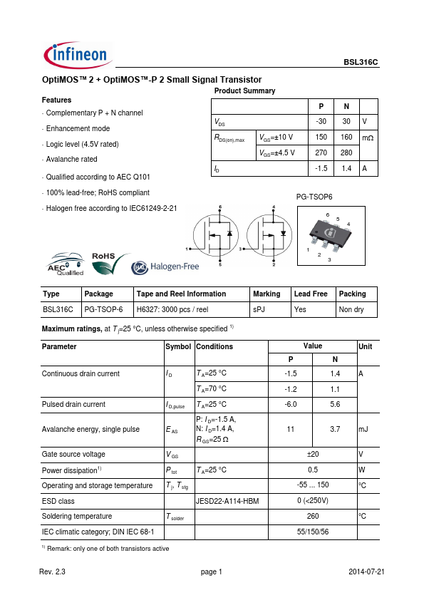
PG-TSOP6
6 5 4
1 2 3
Type
Package
BSL316C PG-TSOP-6
Tape and Reel Information H6327: 3000 pcs / reel
Marking sPJ
Lead Free Packing Yes Non dry
Maximum ratings, at T j=25 °C, unless otherwise specified 1)
Parameter
Symbol Conditions
Continuous drain current
I D T A=25 °C
Pulsed drain current
Avalanche energy, single pulse
Gate source
voltage Power dissipation1) Operating and storage temperature
T A=70 °C
I D,pulse T A=25 °C
P: I D=-1.5 A, E AS N: I D=1.4 A,
R GS=25 W
V GS
P tot T A=25 °C
T j, T stg
ESD class
JESD22-A114-HBM
Soldering temperature
T solder
IEC climatic category; DIN IEC 68-1
1) Remark: only one of both transistors active
Value PN -1.5 1.4 -1.2 1.1 -6.0 5.6
Unit A
11 3.7 mJ
±20 0.5 -55 ... 150 0 (<250V) 260 55/150/56
V W °C
°C
Rev. 2.3
page 1
2014-07-21
Parameter
Symbol Conditions
BSL316C
min.
Values typ.
Unit max.
Thermal characteristics
Thermal resistance, junction ambient1)
P R thJA
N
minimal footprint 2)
-
- 250 K/W
Electrical characteristics, at T j=25 °C, unless otherwise specified
Static characteristics
Drain-source breakdown
voltage Gate thres...