www.DataSheet4U.com
Preliminary data
BSO 215 C
SIPMOS ® Small-Signal-Transistor
Features • Dual N- and P -Channel
•
...
www.DataSheet4U.com
Preliminary data
BSO 215 C
SIPMOS ® Small-Signal-Transistor
Features Dual N- and P -Channel
Product Summary Drain source
voltage Drain-Source on-state resistance Continuous drain current
N
P -20 0.1 -3.7 V Ω A
VDS RDS(on) ID
20 0.1 3.7
Enhancement mode
Logic Level Avalanche rated dv/dt rated
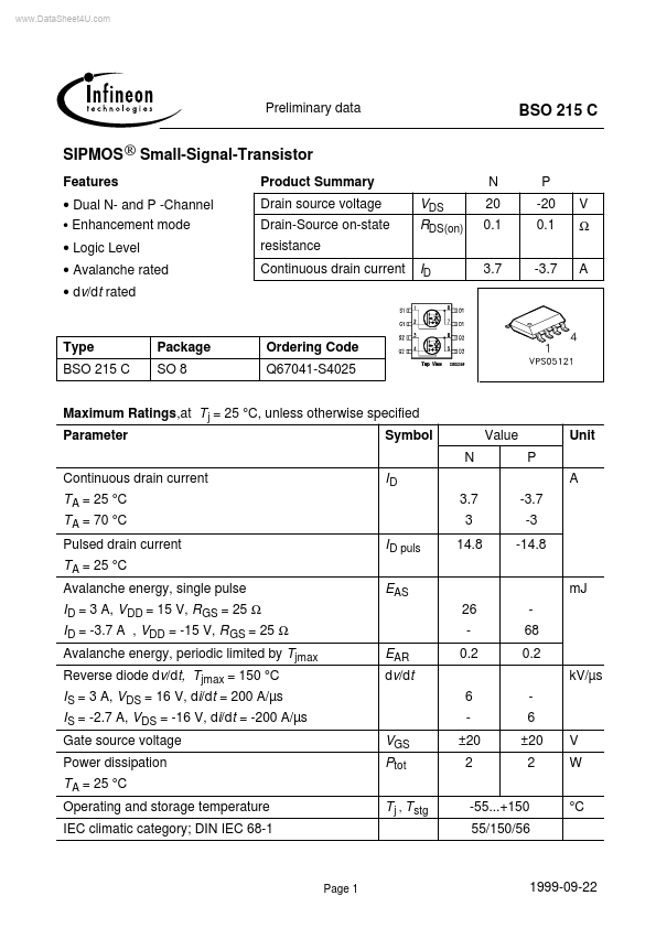
Type BSO 215 C
Package SO 8
Ordering Code Q67041-S4025
Maximum Ratings,at T j = 25 °C, unless otherwise specified Parameter Symbol N Continuous drain current
Value P
Unit A
ID
3.7 3 -3.7 -3 -14.8
T A = 25 °C T A = 70 °C
Pulsed drain current
I D puls EAS
14.8
T A = 25 °C
Avalanche energy, single pulse mJ 26 68 0.2 kV/µs 6 6 ±20 2 V W °C
I D = 3 A, V DD = 15 V, R GS = 25 Ω I D = -3.7 A , VDD = -15 V, R GS = 25 Ω
Avalanche energy, periodic limited by Tjmax Reverse diode dv/dt, T jmax = 150 °C
EAR
dv/dt
0.2
I S = 3 A, V DS = 16 V, di/dt = 200 A/µs I S = -2.7 A, V DS = -16 V, di/dt = -200 A/µs
Gate source
voltage Power dissipation
VGS Ptot T j , T stg
±20 2
T A = 25 °C
Operating and storage temperature IEC climatic category; DIN IEC 68-1 -55...+150 55/150/56
Page 1
1999-09-22
Preliminary data Termal Characteristics Parameter Dynamic Characteristics Thermal resistance, junction - soldering point SMD version, device on PCB: @ min. footprint; t ≤ 10 sec. @ 6 cm 2 cooling area 1) ; t ≤ 10 sec. @ min. footprint; t ≤ 10 sec. @ 6 cm 2 cooling area 1) ; t ≤ 10 sec. N N P P N RthJS P Symbol min.
BSO 215 C
Values typ. max. 40 40 110 62.5 100...